
Custom IC Substrate Manufacturer for 12–30 Layer Designs
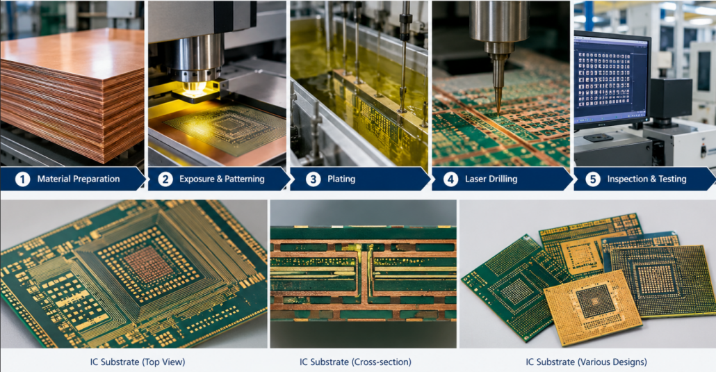
Looking for an IC substrate manufacturer for a complex multilayer design? We provide customized IC substrate solutions for projects requiring 12 to 30 layers, subject to design review and manufacturing feasibility.
Whether you are developing a new semiconductor package or sourcing a custom IC package substrate, we welcome inquiries from engineering teams, semiconductor packaging companies, and electronics manufacturers.
Share your design requirements with us to discuss your custom IC substrate project.
Custom 12–30 Layer IC Substrate Manufacturing
We offer customization for IC substrate designs ranging from 12 to 30 layers, with configurations evaluated according to project-specific requirements.
Multilayer IC substrates require careful consideration of layer construction, electrical interconnections, substrate dimensions, materials, and manufacturing constraints. The appropriate design depends on the intended package architecture and the technical requirements of the application.
Our custom IC substrate service is intended for customers who need substrate configurations tailored to their engineering specifications rather than standard, off-the-shelf products.
Customization Options
- Layer Count: Custom designs from 12 to 30 layers.
- Substrate Dimensions: Project-specific dimensions, subject to manufacturing feasibility.
- Layer Stack-Up: Design requirements reviewed according to the proposed substrate structure.
- Interconnection Design: Via structures and electrical routing evaluated based on the submitted design.
- Application Requirements: Substrate configurations assessed according to the intended semiconductor packaging application.
Final manufacturing feasibility depends on the complete design, material selection, circuit geometry, via structures, and other relevant process requirements.
Have a 12–30 layer IC substrate project? Contact us to discuss your design requirements.
What Is an IC Substrate?
An IC substrate is a specialized substrate used in semiconductor packaging to provide electrical connections between an integrated circuit die and the external circuit board.
It serves as an important part of the package structure, supporting electrical routing, mechanical integration, and connections between different interconnection levels.
Compared with many conventional printed circuit boards, IC substrates may require finer circuit features, higher interconnection density, precise layer alignment, and specialized manufacturing processes.
IC substrates are used in various semiconductor packaging architectures, including BGA and flip-chip packages, depending on the package design and application requirements.
Selecting an appropriate IC substrate involves evaluating the package structure, electrical requirements, dimensions, materials, and reliability expectations.
IC Package Substrate Solutions for Multilayer Designs
An IC package substrate connects the semiconductor die to the next level of electronic assembly. Its design must accommodate the electrical, mechanical, and packaging requirements of the intended device.
For multilayer IC package substrates, the design process may involve:
- Electrical routing and interlayer connections
- Layer stack-up configuration
- Via structures and placement
- Substrate dimensions and thickness
- Material compatibility
- Mechanical stability and package assembly requirements
For 12–30 layer designs, the layer structure should be evaluated as a complete system. Increasing the layer count alone does not guarantee better electrical performance or reliability.
A suitable IC package substrate design depends on the intended application, routing requirements, manufacturing feasibility, and package architecture.
We welcome project inquiries from customers seeking customized multilayer IC package substrates.
Why Work With a Custom IC Substrate Supplier?
Selecting an IC substrate supplier is an important decision for semiconductor packaging projects. Beyond product pricing, customers need to understand whether a supplier can evaluate their design requirements and support the intended manufacturing process.
Application-Specific Customization
Different semiconductor packages require different substrate configurations. Customization allows the layer count, dimensions, and structural requirements to be evaluated according to the project.
Engineering Requirements Review
Before manufacturing, relevant design information should be reviewed to identify potential constraints related to stack-up, materials, routing, vias, and dimensions.
Design-Based Manufacturing Assessment
Manufacturing feasibility depends on the combination of design parameters rather than layer count alone. An engineering review helps establish whether the proposed design is suitable for the available process capabilities.
Clear Communication From Inquiry to Quotation
Providing complete technical information helps reduce uncertainty during project evaluation. Design files, stack-up information, and expected quantities can help the supplier better understand the scope of the project.
When selecting a supplier, customers should also verify relevant quality systems, technical capabilities, certifications, and production experience.
IC Substrate Applications
IC substrates support a range of semiconductor packaging applications. The appropriate substrate structure depends on the device architecture, electrical requirements, and package design.
Potential application categories include:
BGA Package Substrates
Ball Grid Array (BGA) packages use an array of solder balls to connect the package to a printed circuit board. The substrate provides the internal routing required by the package design.
Flip-Chip Package Substrates
Flip-chip packaging connects the die to the substrate through an array of interconnections. Substrate design depends on the die layout, interconnection requirements, and package architecture.
Multilayer Semiconductor Package Substrates
Multilayer configurations support complex routing requirements across multiple conductive layers. The required number of layers depends on the electrical and structural requirements of the application.
If your project requires a custom 12–30 layer IC substrate, share your specifications for an initial manufacturing feasibility discussion.
How to Request a Custom IC Substrate Quote
To help us evaluate your IC substrate project, please provide as much of the following information as is available.
1. Required Layer Count
Specify the target layer count, such as 12, 16, 20, 24, or 30 layers.
2. Substrate Dimensions
Provide the required length, width, and thickness, if already defined.
3. Technical Design Files
Share available design files, stack-up drawings, or other relevant engineering documentation.
4. Material Requirements
Identify any specified substrate materials or material requirements.
5. Application and Package Type
Describe the intended package architecture and application.
6. Project Quantity
Indicate whether the inquiry concerns prototype development, sample quantities, or production requirements.
7. Additional Technical Requirements
Include any specified circuit geometry, via structures, reliability requirements, or other relevant parameters.
Once the available information has been reviewed, the next step is to clarify technical requirements and determine manufacturing feasibility.
[Submit Your IC Substrate Requirements]
Frequently Asked Questions
Can you customize IC substrates from 12 to 30 layers?
We accept inquiries for customized 12–30 layer IC substrate designs. Final feasibility depends on the substrate structure, dimensions, materials, circuit geometry, via design, and other manufacturing requirements.
What is the difference between an IC substrate and a PCB?
An IC substrate is designed specifically for semiconductor packaging and die-to-board interconnection. Compared with many conventional PCBs, IC substrates may require finer circuit features, higher interconnection density, and tighter process control.
What information is needed for an IC substrate quotation?
Useful information includes the layer count, substrate dimensions, thickness, materials, stack-up, design files, application, and expected quantity. Additional specifications may be needed to evaluate manufacturing feasibility.
How do I choose an IC substrate manufacturer?
Evaluate the supplier’s verified layer-count capabilities, relevant process specifications, engineering support, quality systems, certifications, and experience with comparable substrate designs. Confirm that the supplier can meet your specific project requirements.
Are 12–30 layer IC substrates suitable for every semiconductor package?
No. The required layer count depends on the package architecture, routing complexity, electrical requirements, and design constraints. The appropriate structure should be determined through engineering evaluation.
How can I request a quotation for a custom IC package substrate?
Contact us with your target layer count, dimensions, design files, application, and expected quantity. We can use the available information to discuss your requirements and assess the next steps.
Request a Quote for Your Custom IC Substrate


