
Comparing Substrate like PCB SLP with Traditional PCBs
Printed Circuit Boards (PCBs) are the backbone of modern electronic devices, providing the physical platform for electrical components and ensuring reliable connections through conductive pathways. They are essential in various industries, from consumer electronics to automotive and aerospace, due to their ability to enhance device performance, reduce size, and increase reliability.
As electronic devices become more compact and powerful, the demand for advanced PCB technologies has risen. Substrate-like PCB (SLP) represents a significant evolution in this field. SLPs are designed to offer higher density interconnects, improved signal integrity, and enhanced overall performance compared to traditional PCBs. This new trend in PCB technology is driven by the need for smaller, faster, and more efficient electronic devices, making SLPs a critical innovation for the future of electronics manufacturing.
What is Substrate-like PCB (SLP)?
Definition: Substrate-like PCB (SLP) refers to a new class of printed circuit boards that feature finer lines and spaces, higher density interconnects, and advanced microvia technology. Unlike traditional PCBs, SLPs utilize substrate materials and manufacturing techniques more commonly associated with semiconductor packaging. This allows for greater miniaturization and enhanced electrical performance, making SLPs particularly suited for next-generation electronic devices.
Background: The development of SLP technology emerged from the growing need for more compact and efficient electronic components. As consumer electronics, such as smartphones and wearable devices, demand increased functionality within smaller form factors, traditional PCB technologies struggled to keep pace. The concept of SLP was born from advancements in semiconductor packaging, which provided the inspiration for applying similar techniques to PCB fabrication. Over the past decade, significant investments in research and development by leading PCB manufacturers have propelled SLP from a novel concept to a viable and increasingly adopted solution in high-tech industries.
Applications: SLPs are used in a variety of modern electronic products that require high performance and compact designs. In the consumer electronics sector, SLPs are critical for the production of smartphones, tablets, and wearable devices, where space constraints and performance requirements are stringent. In the automotive industry, SLPs enable advanced driver-assistance systems (ADAS) and infotainment systems that demand robust and reliable PCBs with high-density interconnects. Additionally, SLPs are being utilized in medical devices, providing the precision and reliability needed for sophisticated diagnostic and therapeutic equipment. The versatility and superior performance of SLPs are driving their adoption across multiple high-tech applications, solidifying their role as a pivotal technology in the evolution of electronics.
SLP PCB vs. Traditional PCB
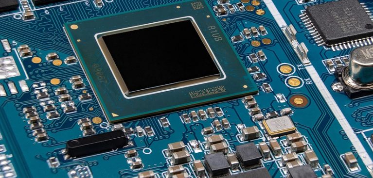
Structural Differences: Traditional PCBs typically consist of multiple layers of copper traces separated by insulating material, with through-hole and surface-mount components attached to them. The line width and spacing in traditional PCBs are relatively larger, which limits the density of components and connections that can be achieved. In contrast, SLPs (Substrate-like PCBs) are designed with finer lines and spaces, often using advanced photolithography and etching processes borrowed from semiconductor manufacturing. This allows for much higher density interconnects and the incorporation of microvias, which are smaller and more efficient than the conventional vias used in traditional PCBs. SLPs often feature multiple layers of high-density interconnect (HDI) technology, providing a more compact and efficient layout.
Performance Differences: The advanced structure of SLPs translates into several performance advantages. Firstly, the higher density interconnects and finer lines and spaces allow for more complex and compact designs, crucial for modern electronics requiring high functionality within limited space. SLPs also offer improved signal integrity and reduced electromagnetic interference (EMI), thanks to their superior material properties and precise manufacturing techniques. The use of microvias and thinner dielectric layers in SLPs reduces the parasitic capacitance and inductance, enhancing the overall electrical performance. This results in faster signal transmission and greater reliability, making SLPs ideal for high-speed and high-frequency applications.
Cost Comparison: While SLPs offer numerous technical advantages, they come at a higher cost compared to traditional PCBs. The advanced materials and sophisticated manufacturing processes required for SLP production contribute to increased costs. The need for precise photolithography and etching techniques, along with the use of high-performance substrate materials, raises the production expenses. Additionally, the complexity of SLP design and fabrication often requires specialized equipment and expertise, further adding to the cost. However, the higher initial investment in SLP technology can be justified by the performance benefits and the potential for integrating more functionality into smaller form factors, which can lead to overall cost savings in the final product assembly and performance enhancement. For applications where performance, miniaturization, and reliability are critical, the benefits of SLPs can outweigh the higher production costs.
Technical Details of SLP
Material Selection: The choice of materials in SLP is crucial for achieving the desired performance characteristics. Common substrate materials used in SLP include high-performance resins and laminates, such as modified epoxy, polyimide, and liquid crystal polymer (LCP). These materials offer excellent thermal stability, low dielectric constant, and low loss characteristics, which are essential for high-speed and high-frequency applications. Additionally, copper foils used in SLPs are often of higher purity and finer grain structure to support the creation of finer lines and spaces. The selection of materials not only affects the electrical performance but also impacts the mechanical strength and reliability of the SLPs.
Manufacturing Process: The manufacturing process of SLPs is more complex and precise compared to traditional PCBs. It begins with the preparation of the substrate material, which is then laminated with a thin layer of copper. Advanced photolithography techniques are used to pattern the copper, creating fine lines and spaces that are much smaller than those in traditional PCBs. Microvias are formed using laser drilling, which allows for precise and reliable interlayer connections. Electroplating and etching processes are employed to define the circuit patterns accurately. One of the significant technical challenges in SLP manufacturing is maintaining the integrity of these fine features throughout the process, as even slight deviations can impact performance. Additionally, ensuring the reliability of microvias, which are critical for high-density interconnects, requires careful control of drilling and plating processes. The use of advanced inspection and quality control methods is essential to meet the stringent requirements of SLP production.
Technical Standards: SLPs must adhere to various technical standards and certifications to ensure quality and reliability. These standards are often defined by industry organizations such as the IPC (Institute for Printed Circuits) and JEDEC (Joint Electron Device Engineering Council). For instance, IPC-6012DA is a specific standard for the qualification and performance specification of high-density interconnect (HDI) structures, which are commonly used in SLPs. Standards like IPC-2226 provide guidelines for the design of HDI circuits. Additionally, SLPs used in critical applications such as automotive and aerospace may need to comply with additional certifications like ISO/TS 16949 for quality management systems in the automotive industry or AS9100 for aerospace applications. Adherence to these standards ensures that SLPs meet the necessary performance, reliability, and safety requirements.
Difference Between SLP and Package Substrate
Definition Comparison
- PCB (Printed Circuit Board): A PCB is a board used to connect electronic components using conductive pathways, tracks, or signal traces etched from copper sheets laminated onto a non-conductive substrate. Traditional PCBs are used in a wide range of electronic devices, providing the foundational platform for component mounting and interconnection.
- SLP (Substrate-like PCB): SLPs are an advanced type of PCB that employs finer lines and spaces, higher density interconnects (HDI), and microvia technology. They use manufacturing techniques similar to those used in semiconductor packaging, allowing for greater miniaturization and enhanced electrical performance compared to traditional PCBs.
- Package Substrate: Package substrates, also known as IC substrates, serve as the intermediary between the silicon die and the PCB. They provide mechanical support, electrical connections, and thermal management for the silicon die. These substrates are integral in semiconductor packaging and are used in applications requiring high performance, such as processors and memory chips.
Application Scenarios
- Traditional PCB: Traditional PCBs are widely used in consumer electronics, industrial equipment, automotive electronics, and many other fields. They are suitable for applications where the size and performance requirements are moderate and where cost considerations are significant. Examples include home appliances, basic computing devices, and simple control systems.
- SLP (Substrate-like PCB): SLPs are used in applications requiring high performance, compact size, and high-density interconnects. They are particularly prevalent in high-end consumer electronics like smartphones, tablets, and wearable devices, where space constraints and performance requirements are critical. SLPs are also used in advanced automotive electronics, including ADAS (Advanced Driver-Assistance Systems) and infotainment systems, as well as in medical devices that require precision and reliability.
- Package Substrate: Package substrates are primarily used in semiconductor packaging, providing the necessary support and interconnections for integrated circuits (ICs). They are crucial in applications demanding high computational power and efficiency, such as processors, memory modules, and high-speed communication devices. Package substrates are also used in advanced microelectronic assemblies, including graphics cards, network routers, and high-performance computing systems.
Related Manufacturers and Technical Capabilities
InPack PCB Technologies: InPack PCB Technologies is a leading manufacturer specializing in advanced PCB solutions, including Substrate-like PCBs (SLPs). They have invested significantly in research and development to enhance their SLP manufacturing capabilities. InPack employs state-of-the-art photolithography and laser drilling techniques to achieve the fine lines and high-density interconnects characteristic of SLPs. Their products are known for excellent thermal management and signal integrity, making them ideal for high-performance applications. InPack’s SLPs are widely used in high-end consumer electronics, automotive systems, and medical devices. Their commitment to innovation and quality has positioned them as a key player in the SLP market, providing customized solutions to meet the specific needs of their clients.
TTM PCB Capabilities: TTM Technologies is one of the world’s largest PCB manufacturers, known for their extensive technical expertise and advanced manufacturing capabilities. TTM has made significant strides in SLP technology, offering products with superior electrical performance, reliability, and miniaturization. Their SLPs feature high-density interconnect (HDI) technology, microvias, and advanced materials that support high-speed and high-frequency applications. TTM’s technical advantages include their ability to handle complex multi-layer designs and integrate various advanced features such as embedded components and thermal management solutions. They serve a broad range of industries, including aerospace, defense, automotive, and telecommunications. Notable application cases include the use of TTM’s SLPs in cutting-edge smartphones, advanced driver-assistance systems (ADAS), and high-performance computing devices.
Viasystems: Viasystems, now part of TTM Technologies, has a rich history of innovation and excellence in PCB manufacturing. They have been at the forefront of developing and implementing SLP technology. Viasystems’ contributions to SLP manufacturing include pioneering techniques in fine line etching, laser microvia drilling, and the use of high-performance substrate materials. Their SLPs are known for their high reliability and performance, meeting the stringent requirements of advanced electronic applications. Representative projects include the development of SLPs for next-generation wearable devices, sophisticated automotive control systems, and high-speed networking equipment. Viasystems’ dedication to quality and technological advancement has made them a trusted partner for companies looking to incorporate SLPs into their products.
Market Prospects and Challenges of SLP
Market Demand:
The demand for Substrate-like PCBs (SLPs) is driven by the rapid evolution of consumer electronics, automotive electronics, and medical devices. As smartphones, tablets, and wearable devices become more compact and feature-rich, the need for SLPs, which offer higher density interconnects and better performance in smaller form factors, is increasing. The automotive industry, particularly with the rise of electric and autonomous vehicles, requires advanced PCBs to support sophisticated systems like ADAS (Advanced Driver Assistance Systems) and infotainment systems. The medical field also benefits from SLPs in the development of compact, high-precision diagnostic and therapeutic devices. Market analysts project a robust growth potential for SLPs, with significant investments from major PCB manufacturers to expand their SLP production capabilities. The global SLP market is expected to grow at a CAGR of over 10% in the next five years, reflecting strong demand across various high-tech sectors.
Technical Challenges:
Despite the promising market prospects, SLPs face several technical challenges. One of the primary issues is the complexity of the manufacturing process, which requires advanced equipment and precise control to produce fine lines and microvias without defects. Maintaining high yields in SLP production is challenging due to the delicate nature of the processes involved. Another significant challenge is ensuring the reliability and durability of SLPs, especially in applications that involve extreme environmental conditions or mechanical stress. Additionally, integrating SLPs with other components in densely packed electronic assemblies requires careful consideration of thermal management and signal integrity. Overcoming these technical hurdles is essential for the widespread adoption of SLP technology.
Future Trends:
The future of SLP technology looks promising, with several potential breakthroughs and trends on the horizon. One major trend is the continued miniaturization of electronic devices, which will drive the need for even finer lines and higher density interconnects in SLPs. Advances in photolithography and laser drilling technologies are expected to support these requirements, enabling the production of SLPs with even smaller feature sizes. Another trend is the integration of SLPs with advanced materials, such as flexible and stretchable substrates, to support emerging applications in wearable electronics and flexible displays. Additionally, the development of more robust and efficient thermal management solutions will enhance the performance and reliability of SLPs in high-power applications. The ongoing research and development efforts by leading PCB manufacturers and the adoption of industry standards will further accelerate the evolution of SLP technology. The convergence of these trends and technological advancements will solidify SLPs as a critical component in the next generation of electronic devices.
FAQs About substrate like pcb slp
Printed Circuit Board (PCB):
Definition: A PCB is a board used to connect electronic components using conductive pathways, tracks, or signal traces etched from copper sheets laminated onto a non-conductive substrate. PCBs are used in various electronic devices and systems.
Structure: Traditional PCBs consist of multiple layers of copper traces separated by insulating material. They typically have larger line widths and spaces, limiting the density of components and connections.
Applications: Widely used in consumer electronics, industrial equipment, automotive electronics, and more, where moderate size and performance requirements suffice.
Substrate-like PCB (SLP):
Definition: SLPs are an advanced type of PCB that features finer lines and spaces, higher density interconnects (HDI), and microvia technology. They use manufacturing techniques similar to semiconductor packaging.
Structure: SLPs have a more compact design with finer lines and higher density interconnects, allowing for greater miniaturization and improved performance.
Applications: Used in high-end consumer electronics like smartphones, tablets, wearable devices, advanced automotive electronics, and medical devices, where high performance and compact size are critical.
Substrate-like PCB (SLP):
Definition: An SLP is a type of PCB that incorporates advanced manufacturing techniques to achieve finer lines, higher density interconnects, and microvia technology. These techniques are similar to those used in semiconductor packaging, enabling greater miniaturization and enhanced electrical performance.
Purpose: Designed to meet the demands of modern electronics that require high functionality in smaller form factors.
Features: Utilizes advanced materials, photolithography, and laser drilling to create high-density interconnects and microvias.
SLP PCB (Substrate-like PCB):
Definition: An SLP PCB is a PCB that uses advanced fabrication methods to achieve a structure similar to semiconductor substrates, with fine lines, high-density interconnects, and microvias. This allows for increased component density and improved performance.
Applications: Ideal for use in high-performance and compact electronic devices such as smartphones, tablets, wearables, automotive systems, and medical devices.
Printed Circuit Board (PCB):
Function: Provides the physical platform for mounting and interconnecting electronic components using conductive pathways etched from copper sheets.
Structure: Consists of multiple layers of copper traces separated by insulating materials, used in various electronic devices.
Package Substrate:
Function: Serves as the intermediary between the silicon die and the PCB, providing mechanical support, electrical connections, and thermal management for the silicon die.
Structure: More complex and smaller in scale compared to PCBs, designed to handle the high-density interconnects and performance requirements of semiconductor packaging.
Applications: Used in semiconductor packaging for components like processors, memory chips, and other high-performance ICs, where precise and reliable connections are essential.

