
Efficiency Redefined: FC QFN Packaging Solutions
In the realm of electronics, packaging plays a pivotal role, acting as the interface between semiconductor devices and their environment. It ensures protection, thermal management, and electrical connections critical for device functionality. Among the modern packaging solutions, FC QFN (Flip Chip Quad Flat No-Lead) packages stand out for their innovative design and performance. These packages offer a compact, leadless structure, optimizing space utilization while enhancing thermal dissipation and electrical performance. As electronics continue to evolve, the importance of advanced packaging solutions like FC QFN becomes increasingly apparent, driving efficiency, reliability, and miniaturization in electronic devices.
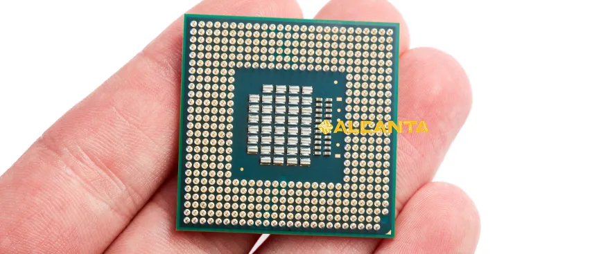
Understanding QFN Packages
Definition and Significance:
QFN (Quad Flat No-Lead) packages represent a significant advancement in semiconductor packaging technology. They are characterized by their leadless design, which enhances thermal and electrical performance while reducing package size. QFN packages play a crucial role in modern electronics by providing a reliable and efficient solution for mounting semiconductor devices onto printed circuit boards (PCBs). Their significance lies in their ability to meet the increasing demands for miniaturization, thermal management, and high-density integration in electronic devices.
Basic Structure and Design:
A typical QFN package consists of a leadframe with the semiconductor die mounted on a metal pad, which serves as both the thermal and electrical contact. The leads are absent in QFN packages, and the external connections are made through exposed metal pads on the bottom surface of the package. These pads enable direct soldering to the PCB, contributing to improved electrical performance and thermal dissipation. Additionally, QFN packages often feature a plastic encapsulation for protection against environmental factors and mechanical stress.
Comparison with Other Packaging Types:
Compared to traditional packaging types like DIP (Dual Inline Package), SOP (Small Outline Package), and BGA (Ball Grid Array), QFN packages offer several advantages. They have a smaller footprint and lower profile, making them suitable for applications where space is limited. QFN packages also provide better thermal conductivity due to the direct connection between the die and the PCB, reducing the risk of overheating. Additionally, their leadless design simplifies the manufacturing process and enhances reliability by minimizing solder joint failures. Overall, QFN packages excel in meeting the demands of modern electronics, outperforming traditional packaging types in various aspects.
Types of QFN Packages
Overview of Different Types:
QFN packages come in various configurations to cater to diverse application requirements, offering flexibility in size, lead count, and thermal characteristics. They are classified based on parameters such as package dimensions, pad pitch, and thermal performance. Variants of QFN packages include standard QFN, micro QFN, and enhanced QFN, each offering unique features suited for specific applications.
Explanation of Types:
1. Standard QFN:
– Standard QFN packages are the most common variant, featuring a typical pad pitch ranging from 0.4mm to 0.8mm.
– They are available in various sizes, with lead counts typically ranging from 8 to 144.
– Standard QFN packages offer good thermal performance and are widely used in consumer electronics, telecommunications, and automotive applications.
2. Micro QFN:
– Micro QFN packages are characterized by smaller dimensions and finer pitch compared to standard QFN packages.
– They typically have a pad pitch of less than 0.4mm, enabling higher lead counts in smaller footprints.
– Micro QFN packages are ideal for compact devices where space-saving is critical, such as wearable electronics, IoT devices, and mobile gadgets.
3. Enhanced QFN:
– Enhanced QFN packages incorporate additional features to improve thermal dissipation and electrical performance.
– These packages may include features such as exposed thermal pads, enhanced lead frames, or specialized materials for better heat dissipation.
– Enhanced QFN packages are commonly used in high-power applications, RF (Radio Frequency) devices, and LED lighting, where efficient thermal management is essential for optimal performance.
Overall, the different types of QFN packages provide designers with a range of options to address specific design constraints and performance requirements, making them versatile solutions for a wide range of electronic applications.
Advantages of QFN Packages
Compact Size and Space-saving Design Benefits:
QFN packages offer a significant advantage in terms of space utilization due to their compact size and leadless design. By eliminating traditional leads, QFN packages achieve a higher component density on the PCB, allowing for more functionality in smaller form factors. This compactness is particularly beneficial in applications where space constraints are critical, such as mobile devices, IoT sensors, and wearable electronics.
Improved Thermal Performance and Reliability:
One of the key advantages of QFN packages is their enhanced thermal performance. The direct thermal path between the semiconductor die and the PCB enables efficient heat dissipation, minimizing the risk of overheating and ensuring the reliability of the device. Additionally, QFN packages often feature exposed thermal pads or enhanced lead frames, further enhancing their thermal conductivity and reliability, particularly in high-power applications and harsh operating environments.
Enhanced Electrical Performance and Signal Integrity:
QFN packages offer superior electrical performance and signal integrity compared to traditional leaded packages. The short interconnect lengths between the semiconductor die and the PCB reduce parasitic capacitance and inductance, leading to improved high-frequency performance and signal integrity. This makes QFN packages well-suited for applications requiring high-speed data transmission, such as telecommunications, networking equipment, and automotive electronics.
Cost-effectiveness in Manufacturing and Assembly Processes:
QFN packages are known for their cost-effectiveness in manufacturing and assembly processes. Their leadless design simplifies the assembly process by eliminating the need for lead forming and insertion, reducing manufacturing complexity and cost. Furthermore, the absence of leads reduces the risk of solder joint failures, improving yield rates and reducing the likelihood of rework or repair. Overall, QFN packages offer a cost-effective solution for electronic manufacturers without compromising on performance or reliability.
Disadvantages of QFN Packages
Susceptibility to Solder Joint Cracking due to Thermal Cycling:
One notable disadvantage of QFN packages is their susceptibility to solder joint cracking, particularly under thermal cycling conditions. The mismatch in coefficient of thermal expansion (CTE) between the semiconductor die, the PCB, and the solder material can lead to mechanical stresses during temperature variations. Over time, these stresses may cause fatigue and ultimately result in solder joint failures, compromising the reliability of the device. Proper design considerations, such as the use of appropriate solder materials and optimizing the PCB layout for thermal management, can help mitigate this issue.
Limited Accessibility for Rework and Repair:
Another challenge associated with QFN packages is their limited accessibility for rework and repair. Unlike traditional leaded packages where leads are exposed and accessible, QFN packages have their connections located beneath the package body, making them difficult to access for rework or repair operations. This limitation can pose challenges in situations where components need to be replaced or repaired, potentially leading to higher costs and longer downtime during the manufacturing or maintenance process.
Challenges in Inspection and Testing Compared to Leaded Packages:
QFN packages present challenges in inspection and testing compared to leaded packages, primarily due to their leadless design and hidden solder connections. Visual inspection of solder joints is more challenging with QFN packages, as the connections are concealed beneath the package body. This can make it difficult to identify defects such as insufficient solder, bridging, or voiding during manufacturing. Additionally, traditional testing methods such as flying probe or bed-of-nails testing may not be as effective for QFN packages, requiring alternative testing techniques such as automated optical inspection (AOI) or X-ray inspection to ensure quality and reliability.
Despite these disadvantages, proper design considerations, manufacturing processes, and testing methodologies can help mitigate the challenges associated with QFN packages, ensuring their successful integration into electronic devices.
Applications of FC QFN Packages
Overview of Industries and Applications:
FC QFN (Flip Chip Quad Flat No-Lead) packages find widespread use across various industries due to their compact size, excellent thermal performance, and reliability. Some of the key industries and applications where QFN packages are commonly used include consumer electronics, automotive, aerospace, and medical devices.
Examples of Applications:
1. Consumer Electronics:
– Smartphones and Tablets: QFN packages are extensively used in smartphones and tablets for components such as microcontrollers, power management ICs, and RF modules, thanks to their compact size and high performance.
– Wearable Devices: Wearable electronics, such as fitness trackers, smartwatches, and hearables, utilize QFN packages for their small form factor, low power consumption, and robustness.
2. Automotive:
– Engine Control Units (ECUs): QFN packages are employed in ECUs for functions like engine management, transmission control, and safety systems, where reliability and thermal performance are crucial.
– Advanced Driver Assistance Systems (ADAS): QFN packages are used in ADAS applications for components like radar sensors, camera modules, and LiDAR systems, enabling features such as collision avoidance, lane departure warning, and autonomous driving.
3. Aerospace:
– Avionics: QFN packages are utilized in avionics systems for functions like flight control, navigation, and communication, where reliability, ruggedness, and high temperature operation are essential.
– Satellite and Spacecraft Electronics: QFN packages are employed in satellite and spacecraft electronics for onboard processing, data handling, and communication systems, offering lightweight and reliable solutions for space missions.
4. Medical Devices:
– Implantable Medical Devices: QFN packages are used in implantable medical devices such as pacemakers, neurostimulators, and implantable drug delivery systems, providing compact and reliable solutions for long-term implantation.
– Medical Imaging Equipment: QFN packages find applications in medical imaging equipment like MRI machines, CT scanners, and ultrasound systems, where high-performance electronics are required for image processing and signal conditioning.
In summary, FC QFN packages are integral components in a wide range of industries and applications, contributing to the advancement of technology and innovation in various fields. Their versatility, reliability, and compact design make them ideal solutions for demanding electronic systems across different sectors.
Future Trends and Developments
Potential Advancements Addressing Current Limitations:
1. Advanced Materials: Researchers are exploring new materials with improved thermal conductivity and mechanical properties to address the solder joint cracking issue in QFN packages. Nanomaterials and composite materials show promise in enhancing the reliability and lifespan of QFN packages under thermal cycling conditions.
2. Rework and Repair Solutions: Innovations in rework and repair techniques are being developed to overcome the limited accessibility of QFN packages. Automated rework systems utilizing robotics and machine vision technology are being introduced to enable precise and efficient rework of QFN packages, reducing costs and downtime.
3. Advanced Inspection and Testing Methods: There is a growing emphasis on the development of advanced inspection and testing methods tailored for QFN packages. Machine learning algorithms and artificial intelligence are being utilized to enhance defect detection accuracy in QFN packages, improving the quality and reliability of electronic assemblies.
Predictions for the Future of QFN Packaging in the Electronics Industry:
1. Increased Adoption in High-Performance Applications: With ongoing advancements in materials and manufacturing processes, QFN packages are expected to gain further traction in high-performance applications such as 5G telecommunications, automotive electrification, and artificial intelligence (AI) systems. The compact size, excellent thermal performance, and high reliability of QFN packages make them well-suited for demanding electronic systems in these emerging fields.
2. Integration with Advanced Technologies: QFN packages are likely to be integrated with emerging technologies such as 3D packaging, heterogeneous integration, and system-in-package (SiP) solutions to enable higher levels of integration and functionality in electronic devices. This integration will facilitate the development of smaller, more powerful, and energy-efficient electronics for a wide range of applications.
3. Focus on Sustainability and Environmental Impact: There is a growing emphasis on sustainability and environmental impact in the electronics industry. Future developments in QFN packaging are expected to prioritize eco-friendly materials, recyclability, and energy efficiency to minimize the environmental footprint of electronic devices. This trend aligns with the industry’s efforts to promote sustainable practices and reduce electronic waste.
In conclusion, the future of QFN packaging in the electronics industry is promising, with ongoing advancements addressing current limitations and driving innovation in materials, manufacturing processes, and integration techniques. As electronic devices continue to evolve, QFN packages are poised to play a crucial role in enabling compact, reliable, and high-performance electronic systems across various sectors.
FAQs about fc qfn package
QFN stands for Quad Flat No-Lead. QFN packages are a type of surface-mount semiconductor package characterized by a flat body with no leads extending from the sides. Instead, the package has exposed metal pads on the bottom surface for electrical connections, offering a compact and space-saving design.
There are several types of QFN packages based on variations in size, lead count, and thermal characteristics. Some common types include standard QFN, micro QFN, and enhanced QFN packages. Standard QFN packages have typical pad pitches ranging from 0.4mm to 0.8mm, while micro QFN packages feature smaller dimensions and finer pitches. Enhanced QFN packages incorporate additional features to improve thermal dissipation and electrical performance.
QFN packages have a few disadvantages, including susceptibility to solder joint cracking due to thermal cycling. The hidden solder connections beneath the package body can make rework and repair challenging. Additionally, QFN packages may pose challenges in inspection and testing compared to leaded packages due to their leadless design and concealed solder joints.
A QFN package typically consists of a leadframe with a semiconductor die mounted on a metal pad. The package body is flat with no leads extending from the sides. Instead, the bottom surface of the package features exposed metal pads for electrical connections. The leads are absent in QFN packages, and the connections are made directly to the PCB. QFN packages often include a plastic encapsulation for protection against environmental factors and mechanical stress.

