
Unveiling Ajinomoto ABF Substrates: Revolutionizing the Semiconductor Industry
Ajinomoto ABF substrates represent a cutting-edge advancement in semiconductor manufacturing. These substrates, developed by Ajinomoto Fine-Techno, offer unparalleled performance and reliability, revolutionizing the way electronic devices are produced. ABF substrates play a crucial role in semiconductor manufacturing processes, serving as the foundation for integrated circuits and electronic components. Their significance lies in their ability to provide high-density interconnections, superior thermal management, and enhanced electrical properties, ultimately enabling the creation of smaller, faster, and more energy-efficient devices. As the demand for advanced electronics continues to rise, the importance of ABF substrates in driving innovation and meeting industry requirements cannot be overstated.
Understanding Ajinomoto ABF Substrates
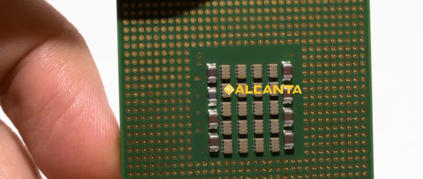
Ajinomoto Build-Up Film (ABF) substrates represent a sophisticated class of materials at the forefront of semiconductor packaging technology. These substrates are engineered with precision to meet the demanding requirements of modern electronic devices.
Definition of ABF Substrates:
ABF substrates are thin layers of dielectric material, typically made from polyimide or liquid crystal polymer, onto which circuit patterns are formed. These substrates serve as the foundation for mounting and interconnecting semiconductor chips within electronic devices.
Composition and Structure:
ABF substrates consist of multiple layers of dielectric material, conductive traces, and vias. The dielectric layers provide insulation between conductive traces and offer mechanical support to the structure. Conductive traces are patterned on the surface to create interconnections between semiconductor chips and other electronic components. Vias are holes drilled through the substrate to establish electrical connections between different layers.
Unique Properties and Advantages:
1. High Density Interconnections: ABF substrates allow for the creation of intricate wiring patterns with high-density interconnections, enabling the integration of more functionality within smaller form factors.
2. Excellent Signal Integrity: The low dielectric constant of ABF materials minimizes signal loss and crosstalk, ensuring reliable transmission of electrical signals.
3. Enhanced Thermal Management: ABF substrates exhibit superior thermal conductivity, dissipating heat efficiently and maintaining optimal operating temperatures for semiconductor devices.
4. Flexibility and Reliability: ABF substrates offer flexibility in design and manufacturing, accommodating various package sizes and configurations. Additionally, their robust construction ensures long-term reliability under harsh operating conditions.
5. Cost-Effectiveness: Despite their advanced features, ABF substrates offer cost advantages over traditional substrates, making them an attractive choice for mass production.
In summary, Ajinomoto ABF substrates stand out for their advanced composition, unique properties, and numerous advantages over conventional materials, making them indispensable in the quest for smaller, faster, and more reliable electronic devices.
Exploring the Technology Behind ABF Substrates
Ajinomoto Fine-Techno’s Role in Developing ABF Substrates:
Ajinomoto Fine-Techno stands as a pioneer in the development and refinement of ABF substrates, leveraging decades of expertise in materials science and semiconductor packaging. Through rigorous research and development efforts, Ajinomoto Fine-Techno has continually pushed the boundaries of innovation, striving to meet the evolving demands of the semiconductor industry. Their collaboration with leading semiconductor manufacturers and research institutions has facilitated the optimization of ABF substrate designs and manufacturing processes, ensuring the delivery of high-performance solutions to the market.
Innovations in Manufacturing Processes:
The production of ABF substrates involves a series of advanced manufacturing processes, each meticulously engineered to achieve superior performance and reliability. Innovations in material deposition, lithography, and etching techniques enable the precise patterning of conductive traces and vias on ultra-thin dielectric layers. Furthermore, advancements in bonding and lamination technologies ensure the integrity and stability of multi-layered structures. Ajinomoto Fine-Techno’s commitment to continuous improvement drives the adoption of state-of-the-art equipment and methodologies, resulting in the consistent delivery of high-quality ABF substrates.
Enhancing Performance and Reliability:
ABF substrates play a critical role in enhancing the performance and reliability of semiconductor devices in several ways:
1. Optimized Signal Transmission: The precise layout of conductive traces and vias minimizes signal distortion and interference, ensuring high-speed and high-fidelity data transmission.
2. Efficient Thermal Management: ABF substrates exhibit excellent thermal conductivity, efficiently dissipating heat generated by semiconductor devices. This helps maintain optimal operating temperatures, preventing performance degradation and extending device lifespan.
3. Mechanical Stability: ABF substrates offer exceptional mechanical stability and durability, withstanding mechanical stress and environmental factors such as temperature variations and humidity. This ensures the long-term reliability of semiconductor packages in demanding applications.
4. Miniaturization and Integration: The compact design of ABF substrates enables the miniaturization of electronic devices while accommodating complex circuitry and multiple semiconductor chips. This facilitates the integration of advanced features and functionality within smaller form factors, meeting the demands of modern consumer electronics and IoT applications.
In conclusion, Ajinomoto Fine-Techno’s relentless pursuit of technological excellence, coupled with innovative manufacturing processes, has enabled the development of ABF substrates that significantly enhance the performance, reliability, and functionality of semiconductor devices. These substrates continue to drive innovation in the semiconductor industry, paving the way for the development of next-generation electronic products.
Applications of ABF Substrates
Utilization in Various Electronic Devices:
ABF substrates find widespread application across a diverse range of electronic devices, including smartphones, laptops, tablets, wearables, and IoT (Internet of Things) devices. In smartphones and tablets, ABF substrates enable the integration of high-performance processors, memory modules, and connectivity components within compact form factors, contributing to enhanced functionality and improved user experience. Similarly, in IoT devices, ABF substrates facilitate the integration of sensors, microcontrollers, and wireless communication modules, enabling seamless connectivity and data processing in smart home, industrial automation, and healthcare applications.
Impact on the Automotive and Aerospace Industries:
The automotive and aerospace industries are increasingly reliant on ABF substrates to meet the demanding requirements of modern vehicle and aircraft systems. In automotive applications, ABF substrates are used in advanced driver assistance systems (ADAS), infotainment systems, engine control units (ECUs), and electric vehicle (EV) powertrain components. These substrates provide the necessary reliability, thermal management, and signal integrity for critical electronic systems in vehicles, contributing to safety, efficiency, and performance improvements. Similarly, in aerospace applications, ABF substrates enable the development of lightweight, high-performance avionics systems, flight control systems, and communication systems, supporting the aerospace industry’s pursuit of greater efficiency, reliability, and connectivity in aircraft platforms.
Potential for Future Advancements in Emerging Technologies:
The versatility and adaptability of ABF substrates position them as key enablers of future advancements in emerging technologies. As the demand for smaller, faster, and more energy-efficient electronic devices continues to grow, ABF substrates offer unparalleled opportunities for innovation in areas such as artificial intelligence (AI), machine learning, augmented reality (AR), and quantum computing. These substrates can support the integration of advanced semiconductor technologies, such as 3D integration, heterogeneous integration, and advanced packaging techniques, paving the way for breakthroughs in performance, scalability, and functionality. Furthermore, ABF substrates hold promise for applications in emerging fields such as flexible electronics, stretchable electronics, and bioelectronics, opening up new possibilities for wearable devices, medical implants, and human-machine interfaces.
In summary, the versatile applications of ABF substrates across various electronic devices, their significant impact on the automotive and aerospace industries, and their potential for driving future advancements in emerging technologies underscore their importance as a foundational technology in the semiconductor industry. As technological innovation continues to accelerate, ABF substrates are poised to play a central role in shaping the future of electronic devices and systems.
Addressing the Shortage of ABF Substrates
Factors Contributing to the Shortage:
Several factors have contributed to the shortage of ABF substrates, impacting the semiconductor industry’s ability to meet growing demand:
1. Rapid Growth in Demand: The increasing demand for electronic devices, driven by trends such as 5G connectivity, IoT adoption, and remote work, has outpaced the capacity of ABF substrate manufacturers to ramp up production.
2. Supply Chain Disruptions: Disruptions in the global supply chain, exacerbated by events such as the COVID-19 pandemic, natural disasters, and geopolitical tensions, have led to delays in raw material procurement, manufacturing, and logistics, affecting ABF substrate production.
3. Complex Manufacturing Processes: The intricate manufacturing processes involved in producing ABF substrates, including precise patterning, multi-layer deposition, and stringent quality control, present challenges in scaling production to meet demand.
Efforts by Ajinomoto Fine-Techno to Mitigate Shortages:
Ajinomoto Fine-Techno has undertaken proactive measures to address the shortage of ABF substrates and ensure continuity of supply:
1. Capacity Expansion: Ajinomoto Fine-Techno has invested in expanding production capacity and upgrading manufacturing facilities to increase the output of ABF substrates, thereby alleviating supply constraints.
2. Diversification of Suppliers: To mitigate the risk of supply chain disruptions, Ajinomoto Fine-Techno has diversified its supplier base, forging partnerships with multiple suppliers for key raw materials and components.
3. Process Optimization: Ajinomoto Fine-Techno continually optimizes manufacturing processes and adopts advanced technologies to enhance production efficiency, reduce cycle times, and improve yield rates, enabling faster turnaround times and increased output.
4. Collaboration with Customers: Ajinomoto Fine-Techno collaborates closely with customers to understand their requirements, forecast demand, and align production schedules, fostering a proactive and responsive approach to addressing shortages.
Future Strategies to Ensure Sustainable Production and Supply:
Looking ahead, Ajinomoto Fine-Techno is committed to implementing long-term strategies to ensure sustainable production and supply of ABF substrates:
1. Investment in Research and Development: Ajinomoto Fine-Techno will continue to invest in research and development to drive innovation in ABF substrate technology, develop new materials, and optimize manufacturing processes, enhancing productivity and product performance.
2. Supply Chain Resilience: Ajinomoto Fine-Techno will enhance the resilience of its supply chain by diversifying sourcing channels, securing strategic stockpiles of critical materials, and establishing contingency plans to mitigate risks and disruptions.
3. Capacity Expansion and Localization: Ajinomoto Fine-Techno will explore opportunities for further capacity expansion and localization of production facilities in key regions, enabling closer proximity to customers and reducing lead times and transportation costs.
4. Sustainability and Environmental Responsibility: Ajinomoto Fine-Techno is committed to promoting sustainability and environmental responsibility throughout its operations, adopting eco-friendly manufacturing practices, reducing waste, and minimizing carbon emissions.
In conclusion, Ajinomoto Fine-Techno’s proactive efforts to address the shortage of ABF substrates, coupled with future-oriented strategies for sustainable production and supply, underscore its commitment to supporting the semiconductor industry’s growth and innovation agenda. By leveraging technological advancements and fostering collaboration across the supply chain, Ajinomoto Fine-Techno aims to ensure the availability of ABF substrates to meet the evolving needs of customers and enable the continued advancement of electronic devices and technologies.
FAQs about ajinomoto abf substrates
The ABF substrate solution refers to a type of substrate used in semiconductor packaging. It consists of multiple layers of dielectric material, conductive traces, and vias. ABF substrates provide a foundation for mounting and interconnecting semiconductor chips within electronic devices.
ABF Ajinomoto refers to Ajinomoto Fine-Techno’s specific brand or line of ABF substrates. Ajinomoto Fine-Techno is a company specializing in the development and manufacturing of advanced materials for the semiconductor industry, and ABF Ajinomoto represents their offering in the field of ABF substrates.
ABF substrates are typically made of dielectric materials such as polyimide or liquid crystal polymer (LCP). These dielectric materials provide insulation between conductive traces and offer mechanical support to the substrate. Additionally, ABF substrates contain conductive traces and vias made of metals like copper, which facilitate electrical connections between semiconductor chips and other electronic components.
Several factors contribute to the shortage of ABF substrate. These include rapid growth in demand for electronic devices, supply chain disruptions caused by events like the COVID-19 pandemic and natural disasters, and the complexity of manufacturing processes involved in producing ABF substrates. The increasing demand for smaller, faster, and more energy-efficient electronic devices has outpaced the capacity of manufacturers to ramp up production, leading to shortages in the market.


发表评论
Want to join the discussion?Feel free to contribute!