
Maximizing Performance: Insights into 3D IC Substrates
In the ever-evolving landscape of semiconductor technology, packaging has undergone a remarkable journey. From the rudimentary forms of wire-bonded chips to the sophisticated 2D and 2.5D packaging techniques, advancements have continuously driven the industry forward. However, the pinnacle of this evolution lies in 3D Integrated Circuits (ICs). Unlike their predecessors, 3D ICs offer vertical integration, stacking multiple layers of active components, thereby revolutionizing device miniaturization, performance, and energy efficiency. In the era of interconnected devices and burgeoning data demands, 3D ICs stand as the cornerstone, promising unprecedented advancements in modern electronics.
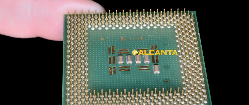
Understanding IC Substrate
Definition and Role of IC Substrate in Semiconductor Devices
The IC substrate serves as the foundation upon which the integrated circuit components are mounted and interconnected. It acts as a support structure, providing mechanical stability and protection to delicate semiconductor materials. Additionally, the substrate facilitates electrical connectivity between the integrated circuit components and the external environment.
Importance of Substrate in Ensuring Electrical Connectivity and Mechanical Support
Electrical connectivity is vital for the proper functioning of semiconductor devices. The substrate plays a crucial role in routing electrical signals between different components of the integrated circuit, ensuring efficient transmission of data and power. Moreover, the substrate provides mechanical support, preventing the integrated circuit components from bending or breaking due to external stresses, such as thermal expansion or mechanical shocks.
Materials Commonly Used in IC Substrate Manufacturing
Various materials are utilized in the manufacturing of IC substrates, each offering unique properties suited for specific applications. Some commonly used materials include:
- Ceramic Substrates: Ceramic substrates, such as alumina (Al2O3) or aluminum nitride (AlN), are known for their excellent thermal conductivity and mechanical strength. They are often used in high-power semiconductor devices and modules.
- Organic Substrates: Organic substrates, typically made of epoxy resins or polyimides, are lightweight and cost-effective. They are commonly used in consumer electronics and low-power applications.
- Glass Substrates: Glass substrates offer high dimensional stability and excellent electrical insulation properties. They are suitable for applications requiring high precision and reliability, such as optical devices and medical implants.
Each material has its advantages and limitations, and the selection depends on factors such as the application requirements, cost considerations, and manufacturing processes.
The Essence of Package Substrate
Definition and Significance of Package Substrate in Semiconductor Packaging
The package substrate, also known as the substrate or interposer, is a crucial component in semiconductor packaging. It serves as a bridge between the integrated circuit (IC) chip and the external environment, providing electrical connectivity and mechanical support. The package substrate is responsible for routing electrical signals between the IC chip and other components, such as interconnects, connectors, and external circuitry. It also dissipates heat generated by the IC chip, ensuring proper thermal management and reliability of the device.
Differentiation between IC Substrate and Package Substrate
While the IC substrate and package substrate are both essential components in semiconductor devices, they serve different purposes. The IC substrate is the base layer upon which the active components of the integrated circuit are mounted and interconnected. It provides electrical connectivity within the IC chip itself. On the other hand, the package substrate is the interface between the IC chip and the external environment. It connects the IC chip to the rest of the device, such as printed circuit boards (PCBs) or other IC chips, and facilitates communication with external devices.
Exploring the Functionalities Served by Package Substrates
- Electrical Interconnection: Package substrates provide pathways for electrical signals to flow between the IC chip and external components. They consist of intricate patterns of conductive traces, vias, and pads that enable the transmission of data and power.
- Signal Integrity: Package substrates play a critical role in maintaining signal integrity by minimizing signal distortion, crosstalk, and noise. Careful design and layout techniques are employed to ensure reliable communication between the IC chip and external devices.
- Thermal Management: Package substrates help dissipate heat generated by the IC chip during operation. They may incorporate features such as thermal vias, metal layers, and heat spreaders to efficiently transfer heat away from the IC chip and prevent overheating.
- Mechanical Support: Package substrates provide mechanical support to the IC chip, protecting it from mechanical stresses and environmental factors. They help to ensure the structural integrity and reliability of the semiconductor device, particularly in harsh operating conditions or during handling and assembly processes.
Overall, package substrates play a vital role in semiconductor packaging, enabling the integration of IC chips into functional devices with reliable electrical connectivity, thermal management, and mechanical support.
Materials Used in IC Packaging
- Ceramic Substrates:
- Ceramic substrates, such as alumina (Al2O3) or aluminum nitride (AlN), are commonly used in IC packaging, especially for high-power applications.
- They offer excellent electrical insulation properties and thermal conductivity, making them suitable for dissipating heat generated by high-power semiconductor devices.
- Ceramic substrates provide good mechanical strength and stability, ensuring reliability in harsh operating conditions.
- Organic Substrates:
- Organic substrates, typically made of epoxy resins or polyimides, are widely used in IC packaging for their lightweight and cost-effectiveness.
- They offer good electrical insulation properties and can be easily manufactured using standard processes, making them suitable for mass production.
- Organic substrates are commonly used in consumer electronics and low-power applications where cost is a critical factor.
- Metal Substrates:
- Metal substrates, such as copper or aluminum, are utilized in IC packaging for their excellent thermal conductivity.
- They are often used in high-power semiconductor devices where efficient heat dissipation is crucial to ensure device reliability and performance.
- Metal substrates may also offer good electrical conductivity, making them suitable for applications requiring high-speed signal transmission.
- Glass Substrates:
- Glass substrates provide high dimensional stability and excellent electrical insulation properties.
- They are commonly used in applications requiring high precision and reliability, such as optical devices and medical implants.
- Glass substrates offer good chemical resistance and can be manufactured with tight tolerances, making them suitable for demanding applications.
Factors Influencing Material Selection
- Electrical Properties:
- The electrical properties of the substrate, such as dielectric constant and electrical conductivity, influence signal integrity and electrical performance.
- Substrates with low dielectric constants and high electrical conductivity are preferred for high-frequency applications to minimize signal loss and distortion.
- Thermal Conductivity:
- The thermal conductivity of the substrate affects its ability to dissipate heat generated by semiconductor devices.
- Substrates with high thermal conductivity are preferred for high-power applications to efficiently remove heat and maintain device reliability.
- Cost-Effectiveness:
- The cost of the substrate material and manufacturing processes is a significant consideration, especially for high-volume applications.
- Materials that offer a good balance of performance and cost-effectiveness are preferred for mass production to ensure competitive pricing and profitability.
Components of 3D ICs
- Through-Silicon Vias (TSVs):
- Through-silicon vias are vertical electrical connections that penetrate through the silicon substrate of individual dies in a 3D IC stack.
- TSVs enable direct communication between stacked dies, reducing interconnect length and signal propagation delay.
- By connecting multiple layers of active components, TSVs facilitate vertical integration, enabling higher device density and enhanced performance.
- Interconnects:
- Interconnects in 3D ICs are horizontal connections that link different functional blocks within the same die or between adjacent dies in a stack.
- These interconnects provide pathways for data transmission, power distribution, and signal routing.
- Advanced interconnect technologies, such as microbumps or copper pillars, are utilized to achieve high-density and high-speed connections, enhancing overall device performance.
- Stacked Dies:
- Stacked dies refer to individual semiconductor chips that are vertically integrated or stacked on top of each other within a single package.
- Each die in the stack contains active components such as transistors, memory cells, or sensors, which perform specific functions.
- Stacking multiple dies enables increased device density, reduced form factor, and improved performance by leveraging the vertical dimension for integration.
Significance of Each Component:
- Through-Silicon Vias (TSVs):
- TSVs play a crucial role in enabling vertical integration by providing direct electrical connections between stacked dies.
- They significantly reduce interconnect lengths and signal propagation delays, enhancing the overall speed and bandwidth of 3D ICs.
- TSVs also contribute to improved power efficiency and thermal management by enabling more efficient power delivery and heat dissipation.
- Interconnects:
- Interconnects enable communication between different layers of stacked dies, facilitating data exchange and signal routing.
- High-density interconnects allow for increased bandwidth and reduced latency, enhancing the overall performance of 3D ICs.
- Optimized interconnect designs contribute to improved signal integrity, reliability, and power efficiency of 3D ICs.
- Stacked Dies:
- Stacked dies enable the integration of multiple functional blocks or heterogeneous components within a compact footprint.
- By stacking multiple dies vertically, 3D ICs achieve higher levels of integration, enabling the implementation of complex systems-on-chip (SoCs) and multi-functional devices.
- Stacked dies also offer opportunities for system-level optimization, such as partitioning critical functions into separate dies for improved performance, scalability, and yield.
Overall, through-silicon vias, interconnects, and stacked dies are integral components of 3D ICs, working synergistically to enable vertical integration, enhance performance, and unlock new capabilities in semiconductor packaging and integration.
Introduction to 2.5D IC Packaging and Its Substrate Requirements
2.5D IC packaging represents an intermediate approach between traditional 2D packaging and full-fledged 3D integration. In 2.5D IC packaging, multiple dies are mounted on an interposer, which serves as an intermediary substrate connecting the individual dies. This interposer, typically made of silicon or organic materials, contains through-silicon vias (TSVs) for vertical connections between the dies.
Comparison with Traditional 2D Packaging and Full-fledged 3D Integration
- Traditional 2D Packaging: In traditional 2D packaging, individual dies are mounted on a single substrate, usually a printed circuit board (PCB). Interconnections between the dies are established using wire bonding or flip-chip bonding techniques. However, this approach has limitations in terms of interconnect density, signal speed, and power efficiency.
- Full-fledged 3D Integration: Full-fledged 3D integration involves stacking multiple dies directly on top of each other, with vertical connections established using through-silicon vias (TSVs). This approach offers maximum integration density and performance but requires complex manufacturing processes and may face challenges in thermal management and yield.
Significance of Package Substrate in Enabling Interposer-based 2.5D Integration
- Interposer as a Bridge: The package substrate, or interposer, plays a critical role in 2.5D IC packaging by serving as a bridge between the individual dies. It provides a platform for mounting and connecting the dies while offering improved electrical performance and signal integrity compared to traditional 2D packaging.
- Enhanced Connectivity: The package substrate enables high-density interconnections between the dies, allowing for increased bandwidth and reduced signal latency. Through the use of TSVs and advanced interconnect technologies, 2.5D IC packaging achieves higher levels of integration and performance compared to traditional approaches.
- Thermal Management: The package substrate also facilitates thermal management in 2.5D IC packaging by providing a platform for integrating thermal dissipation solutions such as heat spreaders or thermal vias. This helps to mitigate thermal hotspots and improve overall device reliability.
2.5D IC packaging leverages the benefits of both 2D and 3D integration approaches, offering increased integration density, improved performance, and enhanced thermal management. The package substrate, particularly the interposer, plays a crucial role in enabling these advancements and serves as a key enabler of interposer-based 2.5D integration.
Comparative Analysis of 2D, 2.5D, and 3D Packaging Approaches
- 2D Packaging:
- In 2D packaging, individual dies are mounted on a single substrate, typically a printed circuit board (PCB), using wire bonding or flip-chip bonding techniques.
- Interconnections between the dies are established on the same plane, limiting integration density and interconnect bandwidth.
- 2D packaging is suitable for low-to-medium complexity applications and offers relatively simple manufacturing processes.
- 2.5D Packaging:
- 2.5D packaging involves mounting multiple dies on an interposer, which serves as an intermediary substrate containing through-silicon vias (TSVs) for vertical connections between the dies.
- This approach enables higher integration density and bandwidth compared to traditional 2D packaging but is less complex and expensive than full-fledged 3D integration.
- 2.5D packaging is suitable for applications requiring increased performance and functionality, such as high-performance computing and networking.
- 3D Packaging:
- In 3D packaging, multiple dies are stacked vertically on top of each other, with through-silicon vias (TSVs) providing vertical connections between the stacked dies.
- This approach offers the highest integration density and performance but requires complex manufacturing processes and may face challenges in thermal management and yield.
- 3D packaging is suitable for applications demanding maximum performance and miniaturization, such as advanced processors, memory devices, and system-on-chip (SoC) designs.
Discussion on the Advantages and Limitations of Each Packaging Paradigm
| Packaging Paradigm | Advantages | Limitations |
| 2D IC Package Substrate | – Simple and cost-effective manufacturing processes. | – Limited integration density and interconnect bandwidth. |
| – Suitable for low-to-medium complexity applications. | – Higher parasitic effects and signal delays. | |
| – Well-established supply chain and infrastructure. | ||
| 2.5D IC Package Substrate | – Higher integration density and bandwidth compared to 2D packaging. | – Complexity and cost associated with interposer fabrication. |
– Reduced form factor and power consumption. | – Challenges in design optimization and signal integrity. | |
– Improved thermal management compared to full-fledged 3D integration. | ||
| 3D IC Package Substrate | – Maximum integration density and performance. | – Complex manufacturing processes and higher fabrication costs. |
– Reduced footprint and power consumption. | – Challenges in thermal management and reliability. | |
– Potential for heterogeneous integration and system-level optimization. |
Importance of Substrate Design and Material Selection
- The substrate design and material selection play a critical role in realizing the potential of each packaging technique.
- For 2D packaging, the substrate material should offer good electrical and thermal properties while being cost-effective.
- In 2.5D packaging, the interposer material must provide high-density interconnects, excellent thermal conductivity, and compatibility with through-silicon via (TSV) fabrication processes.
- In 3D packaging, the substrate material should enable efficient heat dissipation, minimize signal loss, and support the integration of through-silicon vias (TSVs) for vertical connections between stacked dies.
- Advanced substrate materials such as silicon, glass, and organic substrates are commonly used in 2.5D and 3D packaging, each offering specific advantages and limitations depending on the application requirements.
FAQs About 3D IC Package Substrate
The substrate of an IC (Integrated Circuit) is a physical foundation or base upon which the various components of the integrated circuit are mounted and interconnected. It provides structural support and electrical connectivity for the IC.
A package substrate refers to a specific type of substrate used in semiconductor packaging. It serves as a platform for mounting and connecting the IC chip to the rest of the device or external environment. The package substrate facilitates electrical connections between the IC chip and other components, such as interconnects, connectors, and external circuitry.
Various materials are used for IC packaging, depending on the specific requirements of the application. Commonly used materials include ceramic substrates (such as alumina or aluminum nitride), organic substrates (such as epoxy resins or polyimides), and glass substrates. Each material offers unique properties such as electrical conductivity, thermal conductivity, and mechanical strength, which influence its suitability for IC packaging.
The components of 3D ICs (Three-Dimensional Integrated Circuits) typically include through-silicon vias (TSVs), interconnects, and stacked dies. TSVs are vertical electrical connections that penetrate through the silicon substrate of individual dies, enabling communication between stacked dies. Interconnects provide horizontal connections within and between dies. Stacked dies refer to multiple semiconductor chips that are vertically integrated or stacked on top of each other within a single package. These components enable increased integration density, improved performance, and enhanced functionality in 3D ICs.


发表评论
Want to join the discussion?Feel free to contribute!