
What is a PCB Cavity and How It Enhances Circuit Design
PCB cavities are recessed areas within circuit boards that allow components to be embedded at different depths, optimizing space and performance. What is PCB Cavity? It is a key design feature that enhances electrical functionality by reducing signal interference and improving thermal management.
As modern electronics demand thinner and more compact designs, PCB cavities have become essential in high-frequency and high-power applications. They enable better heat dissipation, minimize signal loss, and support the integration of advanced components. Widely used in RF modules, automotive electronics, and miniaturized devices, PCB cavities help achieve high-density layouts without compromising reliability. Their role in optimizing circuit board performance continues to grow as technology advances.
What is a PCB Cavity?
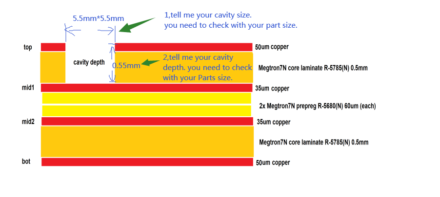
What is PCB Cavity? A PCB cavity is a recessed area within a printed circuit board that allows components to be embedded or placed at different depths, improving space utilization and overall performance. This design feature helps reduce the height of the board and can accommodate components that may not fit on the surface, offering a more compact solution for advanced electronics.
Differences Between Standard PCB Designs and Cavity PCBs
In standard PCB designs, components are typically placed on the surface, with limited options for integrating them into the board. In contrast, cavity PCBs feature recessed areas that enable components to be embedded within the layers of the PCB, offering more flexibility in design. This difference allows cavity PCBs to save space, improve signal integrity, and manage thermal dissipation more efficiently, especially in high-density or high-frequency applications.
Get a Quotation For What is PCB Cavity Now
Applications of PCB Cavities
What is PCB Cavity? It is a recessed area within a PCB that allows components to be embedded at different depths, improving performance and space efficiency. PCB cavities are widely used in various high-tech applications:
RF and Microwave PCBs
PCB cavities help reduce signal interference and improve impedance control, making them essential for high-frequency applications such as wireless communication, radar systems, and satellite technology.
Miniaturized Electronics
Compact devices like smartphones, wearables, and medical implants benefit from PCB cavities, which enable space-saving designs without compromising performance.
High-Power Electronics
By improving thermal dissipation, PCB cavities enhance the reliability of power modules used in automotive electronics, industrial equipment, and energy systems.
Aerospace and Defense
Lightweight, high-performance PCB solutions with cavity structures are critical in avionics, defense systems, and space applications, where reliability and efficiency are paramount.
Get a Quotation For What is PCB Cavity Now
Design Considerations for PCB Cavities
What is PCB Cavity? It is a recessed area within a PCB that allows components to be embedded at different depths, requiring careful design considerations to ensure optimal performance.
Material Selection
Different PCB substrates, such as FR4, ceramic, or glass, affect cavity performance. High-frequency applications benefit from low-loss materials, while thermal-sensitive designs require substrates with excellent heat dissipation properties.
Stack-up Planning
Proper layer arrangement is crucial to maintaining mechanical stability and electrical integrity. Designers must balance cavity depth with overall board thickness to prevent structural weaknesses.
Thermal and Electrical Effects
Cavities influence heat dissipation and signal integrity. Proper thermal management techniques, such as heat vias or thermal pads, help prevent overheating, while careful impedance control minimizes signal loss in high-frequency applications.
Get a Quotation For What is PCB Cavity Now
Advantages and Limitations of PCB Cavities
What is PCB Cavity? It is a recessed area within a PCB that allows components to be placed at varying depths, offering several advantages but also presenting some challenges.
Advantages
-
Space-saving design for compact electronics
PCB cavities allow components to be embedded within the board, reducing the overall height and enabling more compact electronic designs. -
Improved electrical performance
By reducing the length of signal paths, PCB cavities minimize signal loss and interference, enhancing overall performance, especially in high-frequency applications. -
Better thermal management
The ability to integrate components at different depths allows for improved heat dissipation, making PCB cavities ideal for high-power applications where heat management is critical.
Limitations
-
Increased manufacturing complexity and cost
Creating cavities within a PCB requires specialized fabrication techniques like milling, laser drilling, or hybrid methods, increasing both production complexity and cost. -
Potential structural weaknesses in multilayer PCBs
While cavities improve component placement, they can weaken the structural integrity of multilayer PCBs, requiring careful planning to avoid mechanical issues.

