
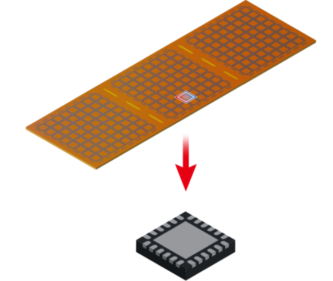
The Role of Ultrathin QFN Lead Frame in Electronics Packaging
In the world of modern electronics, packaging technology plays a crucial role in ensuring the performance, reliability, and miniaturization of electronic components. Lead frames, which are metal frameworks used to connect integrated circuits (ICs) to a printed circuit board (PCB), are a key component in this technology. Among various package types, the QFN (Quad Flat No-lead) package has become increasingly popular due to its compact size, low profile, and enhanced thermal performance. This design eliminates traditional leads, relying instead on solder pads underneath the package for connections. Recently, the demand for even more compact and efficient solutions has given rise to the trend of Ultrathin QFN Lead Frame. This innovation focuses on reducing the overall height of the QFN package while maintaining or improving thermal dissipation and electrical performance. Ultrathin QFN lead frames are particularly well-suited for applications requiring space-saving, such as mobile devices, wearables, and high-density electronics.
What is a QFN Package? Understanding the Structure and Advantages of Ultrathin QFN Lead Frame
A QFN (Quad Flat No-lead) package is a type of surface-mount technology (SMT) package that offers a low-profile, compact form factor with no visible leads. Instead of the traditional wire leads, QFN packages feature flat solder pads located beneath the package, which are directly soldered to the PCB. This unique design eliminates the need for protruding leads, making QFN packages ideal for applications where space is at a premium and height reduction is essential.
Structure and Key Features of QFN Packages
The basic structure of a QFN package consists of a square or rectangular molded plastic body, with a set of leads, or solder pads, underneath. These pads form the electrical connections between the package and the PCB. The lack of external leads helps reduce the overall size and profile of the component, which is why QFN packages are known for their low height. One of the most significant advantages is that the QFN package provides better thermal and electrical performance compared to traditional packages due to the larger surface area for heat dissipation.
The Ultrathin QFN Lead Frame further enhances the QFN package by minimizing its height without compromising performance. This ultrathin version is particularly useful in applications where even smaller, more efficient components are required.
Use Cases of QFN Packages
QFN packages are widely used in various industries, including consumer electronics, automotive, and communications. Their compact and efficient design makes them perfect for mobile devices, tablets, laptops, and wearable technologies, where space is limited, and heat management is critical. In the automotive industry, QFN packages are used in power management systems, sensors, and advanced driver assistance systems (ADAS). Furthermore, the communication sector benefits from QFN’s high-speed signal integrity and low profile, making it an ideal choice for networking devices and telecommunications equipment. With the emerging trend of Ultrathin QFN Lead Frame, these applications are becoming even more miniaturized, driving innovation in smaller, more efficient devices.
Understanding Ultrathin QFN Lead Frames: Design, Manufacturing, and Advantages
The Ultrathin QFN Lead Frame is a specialized variant of the traditional QFN lead frame that focuses on reducing the overall height of the package while maintaining its performance characteristics. This innovation is essential in today’s fast-evolving electronics market, where miniaturization and efficient heat management are paramount.
Thickness of a QFN Lead Frame
A standard QFN lead frame typically has a thickness ranging from 0.3 mm to 0.5 mm. However, Ultrathin QFN Lead Frame versions are significantly thinner, usually falling in the range of 0.15 mm to 0.25 mm. The reduction in thickness is achieved by using advanced manufacturing techniques that allow for the precise shaping and thinning of the metal frame. This ultrathin design is particularly beneficial in applications where height is a critical factor, such as in mobile devices, wearables, or compact automotive electronics.
The thinner lead frame not only reduces the overall height of the package but also contributes to better electrical and thermal performance. By minimizing the package height, the ultrathin design ensures that the component fits into smaller spaces without sacrificing functionality.
Manufacturing Process of Ultrathin QFN Lead Frame
The process of creating an Ultrathin QFN Lead Frame involves advanced stamping, etching, and bonding technologies. Stamping is used to shape the initial metal lead frame, and precision etching techniques are employed to thin the lead frame to the required dimensions. These processes ensure the frame remains strong yet lightweight.
Bonding technologies, such as wire bonding or flip-chip bonding, are used to connect the leads to the IC. The ultrathin design requires careful management of mechanical stresses to avoid potential package failure during assembly or operation. In some cases, copper alloys are used to increase strength without increasing thickness, providing a better balance between performance and structural integrity.
Advantages of Ultrathin QFN Lead Frame
-
Reduced Package Height: One of the primary advantages of the Ultrathin QFN Lead Frame is the significant reduction in package height. This is especially important for applications in mobile electronics and wearables, where space is constrained and slim profiles are necessary.
-
Enhanced Thermal Performance: The ultrathin lead frame design improves heat dissipation compared to traditional packaging solutions. The thinner frame increases the surface area for heat transfer, reducing the likelihood of overheating, which is essential for maintaining performance in high-power or high-frequency applications.
-
Better Reliability in High-Density Applications: With the growing demand for smaller and more powerful electronics, high-density packaging has become a key trend. The Ultrathin QFN Lead Frame offers improved reliability in such applications by enabling more compact, reliable, and thermally stable packages. This is particularly important for devices that must function in harsh environments, like automotive sensors or high-speed communication modules.
The Ultrathin QFN Lead Frame is a technological advancement that offers clear benefits in terms of size, heat management, and performance. These lead frames are essential in driving innovation in modern electronics, where both space and reliability are critical.
The Advantages and Disadvantages of QFN Packages: A Closer Look at Ultrathin QFN Lead Frame
The Ultrathin QFN Lead Frame has revolutionized the QFN (Quad Flat No-lead) package by offering a more compact, thermally efficient, and electrically superior solution. However, like all packaging technologies, QFN packages come with their own set of advantages and challenges. In this section, we’ll explore the key benefits and drawbacks of QFN packages, particularly focusing on how the ultrathin lead frame enhances these attributes.
Advantages of QFN Packages
-
Compact Size
One of the most significant benefits of a QFN package, especially with the Ultrathin QFN Lead Frame, is its compact size. With the lead frame placed beneath the package and the absence of traditional protruding leads, QFNs are much smaller than many other package types, such as BGAs. The ultrathin design further reduces the height of the package, making it ideal for applications where board space is limited, such as in mobile phones, wearables, or other compact consumer electronics. This reduction in size allows for a more efficient and streamlined design in high-density circuit boards. -
Improved Thermal Performance
The Ultrathin QFN Lead Frame provides superior thermal dissipation compared to other packages. The lead frame acts as a heat sink, which helps to dissipate heat generated by the IC. With thinner versions of QFN, such as ultrathin QFN lead frames, the surface area for heat transfer increases, allowing for more efficient heat management in high-power applications. This is crucial in industries like automotive and telecommunications, where managing heat is vital for system reliability and performance. -
Enhanced Electrical Performance
QFN packages, including those with Ultrathin QFN Lead Frame, offer excellent electrical performance. The direct solder pads beneath the package reduce the inductance and resistance between the IC and the PCB, improving signal integrity. Low inductance paths are particularly important for high-frequency applications, where signal integrity must be maintained to prevent degradation. This makes QFNs a preferred choice for applications requiring high-speed data transmission, such as in communication devices and networking equipment. -
Cost-effective
Compared to other packaging options like BGAs (Ball Grid Arrays), QFN packages are typically more cost-effective. The Ultrathin QFN Lead Frame maintains the cost-effectiveness of traditional QFNs, while still offering the advantages of smaller size and better thermal management. Since the assembly process for QFN packages is relatively simple, and there is no need for the specialized equipment required for BGA assembly, the overall cost of production can be lower, making QFNs an attractive choice for manufacturers and consumers alike.
Disadvantages of QFN Packages
-
No Visible Leads
One of the key challenges with QFN packages is that the leads are located underneath the package, making them invisible for inspection. This can complicate the visual inspection process during manufacturing and rework, as traditional inspection methods cannot directly verify the solder joints. However, modern X-ray inspection systems are often used to detect potential issues with the soldering, but these systems are more costly and may not always be available in smaller-scale operations. -
Complex Assembly
The Ultrathin QFN Lead Frame, like other QFN packages, requires precise surface-mount technology (SMT) for assembly. This process demands accurate placement and soldering techniques, as improper soldering can lead to poor connections, which can affect the performance of the entire system. The precision required in the assembly process can make handling QFN packages more complex compared to packages with exposed leads like DIP (Dual In-line Package). Although QFNs are well-suited for automated assembly, the precise nature of the process can still be a challenge for manufacturers. -
Susceptibility to Moisture Sensitivity
Another disadvantage of QFN packages, including Ultrathin QFN Lead Frame, is their susceptibility to moisture sensitivity. Due to the tight construction of the package and the use of plastic molding, QFNs can absorb moisture from the air. If not properly handled and stored in dry conditions, moisture inside the package can vaporize during soldering, leading to the risk of delamination or package cracking. To mitigate this issue, QFN packages must be stored in moisture-controlled environments and may need to be baked before soldering to ensure reliable performance.
While the Ultrathin QFN Lead Frame offers several advantages, such as compact size, enhanced thermal and electrical performance, and cost-effectiveness, there are certain challenges that manufacturers must address, such as the lack of visible leads for inspection, the complexity of the assembly process, and moisture sensitivity. Despite these drawbacks, it remains a valuable choice in applications where size, performance, and cost are key considerations, particularly in high-density and high-performance environments.
Comparing BGA and QFN Packages: Insights into Ultrathin QFN Lead Frame
When it comes to selecting the right package for an electronic component, both BGA (Ball Grid Array) and QFN (Quad Flat No-lead) packages are popular choices. However, there are distinct differences between these two packaging technologies, particularly when we consider the role of the Ultrathin QFN Lead Frame. Here, we’ll compare both package types based on their lead frames, size and profile, thermal and electrical performance, and assembly complexity, highlighting how the ultrathin design in QFN packages offers unique advantages.
Difference in Lead Frames
BGA (Ball Grid Array) packages feature solder balls arranged in a grid pattern on the bottom of the package. These balls act as the interconnects between the package and the PCB. The BGA design allows for a high number of I/O connections in a compact area, making it suitable for high-pin-count applications like processors and memory devices.
In contrast, a QFN package, including the Ultrathin QFN Lead Frame, uses flat pads on the underside of the package for soldering to the PCB. These pads directly connect the IC to the board, eliminating the need for external leads or solder balls. The Ultrathin QFN design further minimizes the package height, offering a more streamlined, low-profile alternative to BGAs, making it ideal for space-constrained designs.
Size and Profile
One of the key differences between BGA and QFN packages lies in their size and profile. BGA packages typically have a larger footprint due to the arrangement of solder balls across the bottom of the package. This makes them ideal for applications that require higher pin counts and larger physical package sizes, such as processors, ASICs, and FPGAs.
QFN packages, especially those with an Ultrathin QFN Lead Frame, are much smaller and thinner. The absence of visible leads and the direct solder pads under the package reduce the overall size, which is critical for applications in smaller devices like smartphones, wearables, and compact automotive electronics. This lead frame enables an even lower profile, making it a strong contender when height reduction is crucial in the design of electronic devices.
Thermal and Electrical Considerations
Thermal management is an important consideration when selecting a package, especially for high-power components. BGA packages tend to offer superior thermal performance due to the solder balls, which are able to transfer heat effectively through the ball-grid structure. This makes BGAs ideal for high-performance processors or applications that generate significant heat.
In contrast, QFN packages rely on the lead frame, including the Ultrathin QFN Lead Frame, to manage heat dissipation. The direct solder pads under the package help channel heat from the IC into the PCB, where it can be spread across larger copper areas. While the Ultrathin QFN design can improve thermal dissipation by increasing the surface area for heat transfer, it may not always provide the same level of heat management as BGA packages. However, for many applications, especially those with lower thermal requirements, the QFN package remains an efficient solution.
From an electrical perspective, both BGA and QFN packages offer excellent performance. However, QFN packages, particularly with the Ultrathin QFN Lead Frame, offer low inductance paths due to the direct solder connections, improving signal integrity. This makes QFNs an attractive option for high-frequency applications where minimal signal interference is required.
Assembly Complexity
When it comes to assembly, QFN packages tend to be simpler to handle, especially with the Ultrathin QFN Lead Frame. The flat solder pads on the bottom of the package can be easily placed using standard surface-mount technology (SMT), which makes the assembly process faster and more cost-effective. Since QFNs do not require any specialized tools for lead or ball placement, their assembly is generally less complex than that of BGAs.
On the other hand, BGA packages require more advanced equipment for the placement of solder balls and their subsequent reflow soldering. This makes BGA assembly more complex and potentially more costly, as it requires precise ball placement, and the use of X-ray inspection is often necessary to ensure the integrity of the solder joints under the package. While BGAs are ideal for high-pin-count applications, the complexity of their assembly makes them less suitable for simpler or cost-sensitive applications compared to Ultrathin QFN Lead Frame packages.
The choice between BGA and QFN packages depends on the specific needs of the application. While BGA packages offer superior thermal performance and higher pin-count capabilities, QFN packages, particularly those with the Ultrathin QFN Lead Frame, excel in smaller, space-constrained designs that require low profile and easy assembly. The Ultrathin design enhances the QFN package by reducing its height, improving thermal dissipation, and simplifying assembly processes, making it an excellent choice for applications in mobile devices, wearables, and other compact electronic systems.
Types of Lead Frames in QFN Packaging: Focus on Ultrathin QFN Lead Frame
QFN (Quad Flat No-lead) packaging has gained widespread use in the electronics industry, particularly due to its efficient use of space and improved thermal and electrical performance. A key component of QFN packages is the lead frame, which provides the electrical connection between the integrated circuit (IC) and the printed circuit board (PCB). There are several variations of the lead frame used in QFN packages, each suited to different types of applications. This section will discuss the main types of lead frames in QFN packaging, including the specialized Ultrathin QFN Lead Frame, which is gaining traction in modern electronic designs.
Standard Lead Frame
The standard QFN lead frame is the most traditional form, typically made from copper or copper alloys. It consists of flat leads that extend from the sides of the package and are arranged in a square or rectangular pattern. These leads are soldered directly to the PCB to form the electrical connections. This basic design is straightforward and provides a reliable solution for a wide range of applications, from power management ICs to sensors.
In the case of Ultrathin QFN Lead Frame designs, the standard lead frame is modified to reduce the overall height of the package without compromising electrical performance. The Ultrathin QFN Lead Frame has a thinner, more compact form, making it ideal for applications where minimizing space is critical, such as in compact consumer electronics.
Microlead Frame (Micro QFN)
The microlead frame, or Micro QFN, is a smaller and thinner version of the standard QFN lead frame. These lead frames are specifically designed for ultra-compact packages and are often used in small-form-factor devices like mobile phones, wearables, and IoT (Internet of Things) devices. Micro QFNs can have even smaller lead pitches (the distance between solder pads), making them ideal for highly miniaturized systems.
While the microlead frame provides a very small package footprint, it also increases the difficulty of assembly due to the need for precise soldering and placement. The Ultrathin QFN Lead Frame variant of this type further reduces the height of the package while retaining its small footprint. The combination of smaller size and low height allows for even more compact, efficient designs, making it suitable for applications where both size and performance are paramount.
Organic Lead Frame
Organic lead frames are made from organic materials, such as resins or polymer composites, rather than traditional metal materials like copper. These organic lead frames are flexible and lightweight, offering distinct advantages for certain applications. They are often used in situations where the package must be thinner, lighter, or more flexible than what traditional metal lead frames can provide. Organic lead frames are increasingly used in specialized industries that require these properties, such as in flexible electronics or medical devices where flexibility and durability are crucial.
The Ultrathin QFN Lead Frame can also be integrated with organic materials for applications that require flexibility along with a low-profile package. In these cases, the organic lead frame reduces the need for rigid metal structures, providing a more versatile packaging solution. The combination of flexibility and ultrathin design enables the development of next-generation electronics that are both compact and adaptable, ideal for wearable technology and other dynamic applications.
Ultrathin QFN Lead Frame
The Ultrathin QFN Lead Frame is the most advanced and specialized version of the QFN lead frame. It is designed specifically for applications where minimizing both size and height is critical, without compromising on thermal or electrical performance. The thickness of the Ultrathin QFN Lead Frame typically ranges from 0.15 mm to 0.25 mm, which is significantly thinner than traditional QFN lead frames.
This ultrathin design is ideal for applications in compact devices like smartphones, tablets, and wearables, where real estate on the PCB is extremely limited. The Ultrathin QFN Lead Frame is especially beneficial in applications that need to reduce height while maintaining good heat dissipation and signal integrity. In addition, the thin lead frame enhances the overall compactness of the package, making it easier to fit more components into smaller spaces without sacrificing performance. The Ultrathin QFN Lead Frame ensures that the components are both small and thermally efficient, making it the go-to solution for space-constrained, high-performance applications.
The Ultrathin QFN Lead Frame represents the cutting edge of QFN packaging technology, offering unparalleled benefits in terms of compact size and low height. Whether in traditional, micro, or organic forms, QFN lead frames play a crucial role in modern electronics, ensuring reliable electrical connections and efficient thermal management. By adopting Ultrathin designs, manufacturers can achieve even more compact and efficient electronic products, which is crucial in today’s fast-paced, miniaturized world of technology. The various types of lead frames in QFN packages, including the Ultrathin QFN Lead Frame, allow designers to select the best solution for their specific needs, driving innovation in a variety of industries.
Key Considerations for Ultrathin QFN Lead Frame Applications: Addressing Thermal, Electrical, and Reliability Challenges
The Ultrathin QFN Lead Frame offers remarkable benefits in terms of compactness and performance, but it also introduces several challenges that must be carefully managed. When designing with these packages, engineers must address thermal management, electrical performance, and reliability concerns to ensure optimal functionality and longevity. In this section, we will discuss these key considerations and potential solutions to overcome the limitations associated with ultrathin designs.
Thermal Management: Addressing Heat Dissipation in Ultrathin Designs
One of the primary challenges of Ultrathin QFN Lead Frame designs is efficient thermal management. As components become smaller and thinner, the heat generated by the IC must still be dissipated effectively to prevent overheating and ensure reliable performance. In traditional QFN packages, the metal lead frame provides a solid thermal path, but when the lead frame is thinned to ultrathin levels (typically between 0.15 mm and 0.25 mm), the overall surface area for heat dissipation is reduced.
Potential Solutions:
- Copper Alloys: One effective solution is the incorporation of copper alloys in the Ultrathin QFN Lead Frame. Copper has excellent thermal conductivity properties, allowing it to better manage heat in ultrathin packages. By using copper or copper-based alloys, manufacturers can ensure that the Ultrathin QFN Lead Frame retains its thermal dissipation capabilities, even with a reduced thickness.
- Thermal vias: Another solution is the use of thermal vias in the PCB itself. These vias provide an additional path for heat to be transferred from the lead frame to the PCB, which helps to spread heat over a larger area and improve overall thermal management. Additionally, embedding heat spreaders within the PCB can further enhance heat dissipation.
- Improved Mold Materials: Using advanced mold compounds with better thermal conductivity can also help in enhancing heat dissipation from the Ultrathin QFN Lead Frame.
Electrical Performance: Ensuring Low Inductance and Resistance
In Ultrathin QFN Lead Frame designs, maintaining excellent electrical performance is essential. Low inductance and resistance are critical for high-speed signal integrity, especially in applications that require fast data transmission or operate at high frequencies. The reduced height of the Ultrathin QFN Lead Frame makes it easier to create low-inductance paths, but the reduced cross-sectional area of the lead frame could increase resistance if not carefully engineered.
Key Considerations:
- Pad Design: Proper pad design on the PCB is crucial to maintaining low inductance and resistance. Ensuring that the pad layout aligns with the lead frame can minimize the distance the signal must travel and help reduce potential signal loss or interference.
- Quality of Materials: The use of high-quality materials for the Ultrathin QFN Lead Frame can improve its electrical performance. For example, using high-purity copper or other materials with low electrical resistance can help ensure that the signal integrity remains intact even in ultrathin designs.
- Solder Joint Integrity: Proper soldering techniques are essential to maintaining low resistance in Ultrathin QFN Lead Frame packages. Ensuring that the solder joints are solid and have good electrical contact is important for minimizing resistance and ensuring reliable signal transmission.
Reliability: Managing Mechanical Stresses and Enhancing Durability
Mechanical reliability is another important consideration for Ultrathin QFN Lead Frame packages. As the lead frame is thinned, it becomes more susceptible to mechanical stresses during both assembly and operation. The reduced thickness can lead to issues such as package warping, crack propagation, or failure under thermal cycling. The Ultrathin QFN Lead Frame must be able to withstand the stresses of assembly (such as soldering) and thermal cycling (due to heating and cooling during operation) without losing integrity.
Key Considerations for Enhancing Reliability:
- Gold-Plated Lead Frames: One way to enhance the mechanical reliability and electrical performance of the Ultrathin QFN Lead Frame is to use gold-plated lead frames. Gold plating not only improves the corrosion resistance of the lead frame but also provides better conductivity than other materials. This can help to maintain signal integrity over time and improve the overall lifespan of the package.
- Stress-Relief Features: Engineers can design the Ultrathin QFN Lead Frame to include stress-relief features, such as reinforced corners or additional support structures, to prevent mechanical failure during thermal cycling or handling. These design adjustments can help distribute mechanical stresses more evenly across the package.
- Materials Engineering: The choice of materials also plays a crucial role in the overall reliability of the Ultrathin QFN Lead Frame. Using alloys with higher fatigue resistance and strength can help mitigate issues with mechanical failure. For example, some QFN packages with ultrathin lead frames use special copper alloys or hybrid materials that enhance the overall structural integrity of the lead frame.
The ultrathin lead frame presents significant advantages in terms of size and performance but requires careful attention to thermal, electrical, and reliability considerations. Addressing heat dissipation challenges through the use of copper alloys or thermal vias, ensuring low inductance and resistance for optimal electrical performance, and improving reliability through gold-plated lead frames and stress-relief features are essential for maximizing the effectiveness of these packages. By addressing these key concerns, manufacturers can fully leverage the benefits of ultrathin designs while maintaining the reliability and performance required in modern electronic applications.
Future Trends in QFN and Lead Frame Technology: The Evolution of Ultrathin QFN Lead Frame
As the demand for more powerful and compact electronic devices continues to grow, the evolution of QFN (Quad Flat No-lead) packaging technology is keeping pace with the need for miniaturization and increased performance. Among the various advancements in QFN packaging, the Ultrathin QFN Lead Frame is at the forefront of enabling smaller, more efficient designs. This section explores the key future trends in QFN and lead frame technology, including miniaturization, the development of advanced materials, and the integration of QFN with other packaging technologies to meet the demands of increasingly complex applications.
Miniaturization: The Drive for Smaller and More Efficient Packages
The trend toward miniaturization remains one of the most significant forces shaping the future of Ultrathin QFN Lead Frame and other semiconductor packaging technologies. As consumer electronics become smaller, lighter, and more integrated, there is a growing need for packaging solutions that can accommodate powerful, multi-functional components in ultra-compact spaces. This technology is a natural fit for this demand, offering reduced height and footprint without sacrificing electrical or thermal performance.
Future generations of Ultrathin QFN Lead Frame packages will likely continue to shrink in size, with thinner lead frames and smaller pad pitches to further reduce the overall height and profile of the package. This trend will enable the development of even more compact devices like smartwatches, advanced wearables, and high-performance smartphones, all of which require high-density packaging solutions that do not compromise on power or heat dissipation.
Advanced Materials: Enhancing Performance in Ultrathin Designs
The development of new materials will be crucial in driving the performance of Ultrathin QFN Lead Frame technology to new heights. Traditional materials like copper and copper alloys have served as the standard for lead frames, but the push for thinner and more efficient packages is driving the exploration of alternative and advanced materials that can improve the mechanical, thermal, and electrical properties of ultrathin designs.
Key Trends in Material Innovation:
- Copper Alloys: Copper remains a top material for lead frames due to its excellent thermal and electrical properties. In the future, new copper alloys designed specifically for ultrathin designs may offer even better thermal conductivity, enabling Ultrathin QFN Lead Frame packages to handle more power while maintaining thermal stability.
- Advanced Polymer Composites: The use of advanced polymers and organic materials in lead frames is also growing. These materials offer flexibility and can be used in applications requiring thinner and more durable packages. For example, hybrid lead frames that combine copper and polymer materials could provide both high conductivity and mechanical resilience, offering a balanced solution for Ultrathin QFN Lead Frame packages in the future.
- Thermally Conductive Coatings: As heat dissipation remains a major concern, researchers are developing thermally conductive coatings that can be applied to the lead frame surface. These coatings can significantly improve heat dissipation from Ultrathin QFN Lead Frame packages, addressing thermal challenges without increasing the package size.
Integration with Other Packaging Technologies: Expanding Functionality in Smaller Footprints
One of the most exciting trends for the future of Ultrathin QFN Lead Frame packaging is its integration with other advanced packaging technologies. As the complexity of electronic devices increases, manufacturers are seeking ways to combine multiple functionalities into smaller and more efficient form factors. QFN packages are well-positioned to integrate with emerging technologies like System-in-Package (SiP) and 3D packaging, enabling the creation of highly integrated, multi-functional devices.
-
System-in-Package (SiP): SiP technology allows for the integration of multiple chips or components within a single package, reducing the size and improving the overall functionality of the device. Combining Ultrathin QFN Lead Frame with SiP enables the integration of various functionalities, such as power management, sensors, and communication modules, into one compact, low-profile package. This combination is particularly beneficial for applications like IoT devices, wearables, and automotive electronics, where space is limited, but high performance is required.
-
3D Packaging: 3D packaging is another promising area for the future of Ultrathin QFN Lead Frame technology. By stacking multiple ICs or components vertically within a single package, 3D packaging increases component density without expanding the footprint. Ultrathin QFN Lead Frame packages, with their low-profile design, are ideal for use in 3D packaging, where space constraints demand that all components fit into a very small volume. Additionally, 3D packaging can improve performance by shortening the interconnect lengths between chips, leading to faster signal transmission and reduced power consumption.
-
Hybrid Package Designs: Future trends may also include hybrid designs that combine Ultrathin QFN Lead Frame packages with other packaging types, such as BGAs (Ball Grid Arrays) or flip-chip packages. These hybrid designs could offer the best of both worlds: the compact, low-profile benefits of QFN with the high I/O capabilities of BGAs or the efficient thermal dissipation of flip-chip designs.
The future of Ultrathin QFN Lead Frame technology is set to be driven by miniaturization, the development of advanced materials, and the integration of multiple packaging technologies to enable more complex functionality in smaller, more efficient devices. As demand grows for high-performance components in ever-shrinking form factors, the Ultrathin QFN Lead Frame will continue to evolve, incorporating new materials for better thermal and electrical performance while supporting advanced packaging techniques like SiP and 3D packaging. These advancements will enable the next generation of electronic devices that are smaller, faster, and more powerful than ever before, while maintaining the high reliability and performance required by today’s demanding applications.
FQAs Abut Ultrathin QFN Lead Frame
How thick is a QFN lead frame?
The typical thickness of a QFN lead frame ranges from 0.25 mm to 0.4 mm. However, for Ultrathin QFN Lead Frame versions, the thickness can be reduced to between 0.15 mm to 0.25 mm, which helps achieve a low-profile design suitable for space-constrained applications.
What are the disadvantages of QFN package?
Some disadvantages of QFN packages include:
- No visible leads: The leads are underneath the package, making visual inspection difficult.
- Complex assembly: Requires precise surface-mount technology (SMT) for soldering, making assembly more complicated.
- Moisture sensitivity: The package needs to be handled and stored carefully to avoid moisture-related issues during reflow soldering, which can degrade the package.
What is the difference between BGA and QFN?
- BGA (Ball Grid Array) uses solder balls on the underside of the package as interconnects, whereas QFN has flat pads that are soldered directly to the PCB.
- Size and Profile: BGA packages typically have a larger footprint and more height compared to the low-profile QFN.
- Thermal and Electrical Considerations: BGA offers better thermal management due to its solder balls, while QFN relies on the lead frame for thermal dissipation.
- Assembly: QFN is easier to place in SMT processes, while BGA may require more advanced equipment for ball placement and reflow soldering.
What are the different types of lead frames?
There are several types of lead frames, including:
- Standard Lead Frame: The traditional QFN lead frame with flat leads.
- Microlead Frame: A smaller, thinner version for ultra-compact designs, used in mobile devices and wearables.
- Organic Lead Frame: Made from organic materials, offering flexibility and used in applications requiring thinner, more flexible packages.
- Ultrathin Lead Frame: Specifically designed for applications where both compact size and low height are critical, with thickness typically ranging from 0.15 mm to 0.25 mm.

