
Printed Circuit Board Substrate Materials for Optimal Performance
Background: Printed Circuit Boards (PCBs) are fundamental components in modern electronic devices, serving as the backbone that supports and electrically connects various electronic components. A PCB consists of multiple layers of conductive pathways embedded in a non-conductive substrate material. These pathways are etched from copper, enabling the circuit to function effectively.
Importance of Topic: The substrate material of a PCB is crucial as it influences the board’s electrical performance, mechanical stability, and thermal management. High-quality substrates ensure optimal electrical insulation, minimal signal interference, and reliable performance under various environmental conditions. Poorly chosen substrates can lead to circuit failures, reduced lifespan, and overall inefficiency. Therefore, understanding different substrate materials and their properties is essential for designing reliable and high-performance PCBs, which are pivotal in ensuring the functionality and longevity of electronic devices.
Overview of PCB Substrate Materials
Definition of PCBs
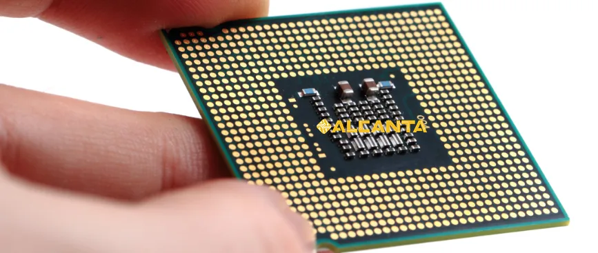
A Printed Circuit Board (PCB) is a critical component in electronic devices, acting as a physical support for electronic components and providing the necessary electrical connections between them. PCBs are made by layering conductive paths, typically copper, onto a non-conductive base material. These paths form the electrical circuit that allows components such as resistors, capacitors, and integrated circuits to function together seamlessly. PCBs are used in a wide array of devices, from consumer electronics like smartphones and computers to industrial machinery and medical equipment. They are essential for ensuring the reliable operation and integration of electronic components within these devices.
Definition of Substrate Materials
PCB substrate materials are the foundational layers upon which the conductive paths and components are built. These materials provide structural support and electrical insulation, ensuring that the circuit functions correctly without interference or mechanical failure. The choice of substrate material affects the PCB’s electrical performance, thermal management, and mechanical properties. Key characteristics of substrate materials include their dielectric constant, thermal conductivity, and mechanical strength. High-quality substrates help maintain signal integrity, manage heat dissipation, and ensure the overall reliability of the PCB. Understanding the different types of substrate materials and their properties is essential for designing PCBs that meet specific performance and durability requirements.
Common Types of PCB Substrate Materials
FR4 Substrate
Description: FR4 is the most widely used PCB material, known for its versatility and reliability. It is composed of a laminate made from woven glass fibers soaked in epoxy resin. This composite material provides a stable and robust foundation for circuit boards, making it suitable for a broad range of electronic applications.
Properties: FR4 substrates offer excellent electrical insulation, which helps prevent short circuits and signal interference. They also possess high mechanical strength, ensuring the PCB can withstand physical stress and mechanical forces. Additionally, FR4 is cost-effective, making it a popular choice for both consumer and industrial electronics. Its moderate cost and reliable performance make it a go-to material for many standard PCB applications.
Insulated Metal Substrate (IMS)
Description: Insulated Metal Substrate (IMS) materials are designed for high-power electronic applications where efficient heat dissipation is crucial. IMS substrates typically feature a metal core, such as aluminum or copper, with a thermally conductive insulating layer.
Properties: The key advantage of IMS substrates is their excellent heat dissipation capabilities. The metal core conducts heat away from sensitive components, reducing the risk of overheating and improving overall reliability. This makes IMS substrates ideal for use in power electronics, LED lighting, and other high-power applications where thermal management is essential.
Ceramic Substrates
Description: Ceramic substrates include materials such as Aluminum Nitride (AlN) and Silicon Nitride (Si3N4). These substrates are used in applications that require high performance under extreme conditions, including high-frequency or high-temperature environments.
Properties: Ceramic substrates offer high thermal conductivity, which enhances their ability to dissipate heat effectively. They also exhibit excellent thermal resistance, allowing them to maintain performance in high-temperature settings. These properties make ceramic substrates suitable for applications in advanced electronics, such as high-frequency RF circuits and high-power components.
Flexible Substrates (Flexible PCB)
Description: Flexible substrates, also known as flexible PCBs, are made from materials like Polyimide (PI) or Polyester (PET) that allow the PCB to be bent or folded. This flexibility enables the PCB to be used in applications where space is constrained or where the board needs to conform to non-flat surfaces.
Properties: Flexible substrates are lightweight and have the ability to be bent or folded without damaging the circuit. This makes them ideal for applications in wearable electronics, medical devices, and compact consumer electronics. Their flexibility and durability offer significant design freedom, allowing for innovative and space-efficient solutions.
High-Frequency Materials (e.g., Rogers 4003c)
Description: High-frequency PCB materials, such as Rogers 4003c, are specifically designed for applications that operate at microwave or radio frequencies. These materials are engineered to minimize signal loss and maintain signal integrity at high frequencies.
Properties: Rogers 4003c and similar materials provide low dielectric loss and a stable dielectric constant, which are critical for high-frequency applications. These properties help ensure that signals are transmitted with minimal attenuation and distortion, making them suitable for high-performance RF and microwave circuits. The stable electrical characteristics of these materials enhance the overall performance of high-frequency electronic devices.
Physical Properties of PCB Substrate Materials
Electrical Performance
Insulation: Electrical insulation is a crucial property of PCB substrates, as it prevents unintended electrical current from flowing between different circuit paths or components. High-quality substrate materials offer superior insulation, which minimizes the risk of short circuits and ensures reliable operation of the PCB. Effective insulation is essential for maintaining circuit integrity and performance, especially in high-density and high-frequency applications.
Dielectric Constant: The dielectric constant of a substrate material indicates how well it can store electrical energy in an electric field. A material with a low dielectric constant helps reduce signal delay and maintain signal integrity, which is particularly important for high-speed and high-frequency circuits. Conversely, materials with high dielectric constants can be used where greater capacitive effects are desired.
Dielectric Loss: Dielectric loss refers to the energy dissipated as heat in the substrate material when an alternating current passes through it. Low dielectric loss is desirable as it reduces signal attenuation and heat generation, which helps in maintaining signal quality and improving the efficiency of the PCB. High-frequency and high-speed applications, in particular, require materials with minimal dielectric loss to ensure optimal performance.
Mechanical Performance
Strength: Mechanical strength defines the substrate’s ability to withstand physical forces without deforming or breaking. A strong substrate material ensures the mechanical stability of the PCB, preventing damage during manufacturing, assembly, and end-use. It is crucial for maintaining the structural integrity of the PCB, especially in applications where mechanical stress is prevalent.
Toughness: Toughness is the ability of a substrate material to absorb impact without cracking or breaking. A tough substrate can endure mechanical shocks and vibrations, which is important for durable and reliable PCBs used in rugged or dynamic environments. Toughness contributes to the overall durability and longevity of the PCB.
Temperature Resistance: Temperature resistance refers to the substrate’s capability to operate and maintain performance under varying temperature conditions. High-temperature resistance is essential for applications that experience significant thermal stress, such as power electronics and automotive components. A substrate with good temperature resistance ensures that the PCB remains functional and stable across a range of temperatures.
Thermal Performance
Thermal Conductivity: Thermal conductivity measures how effectively a material can transfer heat. High thermal conductivity is crucial for dissipating heat generated by electronic components, preventing overheating, and maintaining the reliability of the PCB. Substrates with high thermal conductivity, such as those used in IMS and ceramic materials, are essential for high-power and high-frequency applications.
Coefficient of Thermal Expansion (CTE): The coefficient of thermal expansion indicates how much a material expands or contracts with temperature changes. A substrate with a low CTE is preferable as it minimizes dimensional changes during thermal cycling, reducing the risk of mechanical stress and delamination. Matching the CTE of the substrate with that of other materials in the PCB helps ensure reliable performance and longevity.
Comparison of Different Types of PCB Materials
Rigid PCB vs. Flexible PCB
Substrate Materials: Rigid PCBs typically use FR4 or similar rigid substrates that offer high mechanical strength and durability. These materials are designed to support fixed, stable electronic components and circuits. In contrast, Flexible PCBs use substrates like Polyimide (PI) or Polyester (PET), which are inherently bendable and adaptable to various shapes and forms. These flexible materials are engineered to withstand bending and folding, accommodating dynamic movements or confined spaces.
Application Scenarios: Rigid PCBs are commonly used in applications where stability and durability are paramount, such as in consumer electronics, automotive control systems, and industrial machinery. Their rigidity ensures that components remain securely in place, which is crucial for maintaining circuit integrity. Flexible PCBs, on the other hand, are ideal for applications where space constraints or complex shapes are involved, such as in wearable electronics, flexible displays, and compact devices that require movement or flexibility.
Advantages and Disadvantages:
– Rigid PCBs: Advantages include high structural strength, ease of assembly, and well-established manufacturing processes. Disadvantages may include limited design flexibility and difficulty fitting into compact or irregular spaces.
– Flexible PCBs: Advantages include lightweight, adaptability to complex shapes, and suitability for applications with movement or tight spaces. Disadvantages may include higher cost compared to rigid PCBs and potentially lower mechanical strength and durability.
Standard PCB vs. High-Frequency PCB
Materials: Standard PCBs often use FR4 or similar materials that are cost-effective and provide adequate performance for general electronic applications. These materials offer good electrical insulation, moderate thermal conductivity, and reasonable dielectric properties. High-Frequency PCBs, such as those using Rogers 4003c or other specialized materials, are designed to handle high-frequency signals with minimal signal loss and distortion. They use substrates with low dielectric loss and stable dielectric constants to maintain signal integrity at high frequencies.
Impact on Performance:
– Standard PCBs: Suitable for most general-purpose electronic circuits, providing a good balance of electrical, mechanical, and thermal properties at a lower cost. However, they may not perform well in applications requiring high-speed signal transmission or precision due to higher dielectric loss and signal attenuation.
– High-Frequency PCBs: Designed for applications like RF and microwave circuits, where maintaining signal quality is critical. These PCBs use advanced materials that offer low dielectric loss and stable electrical characteristics, ensuring reliable performance at high frequencies. The higher cost and more complex manufacturing processes are justified by the improved performance and reduced signal degradation.
Overall, the choice between standard and high-frequency PCBs depends on the specific requirements of the application, including performance needs, cost considerations, and design constraints.
PCB Manufacturing Process
Material Preparation
Selecting Substrate Materials: The first step in the PCB manufacturing process is selecting the appropriate substrate materials based on the design requirements and intended application. This involves choosing the right type of substrate material, such as FR4, ceramic, or flexible materials, based on factors like electrical performance, thermal management, and mechanical strength. The chosen material must meet the specifications for dielectric constant, thermal conductivity, and other critical properties.
Processing Substrate Materials: After selecting the substrate material, it is prepared for use in PCB fabrication. This involves cutting the substrate into the required dimensions and sometimes pre-treating it to enhance adhesion between layers. For instance, rigid substrates may need to be cleaned and treated with a chemical primer to ensure proper bonding during lamination. Flexible substrates are typically handled with care to prevent damage during processing.
Lamination
Layering Materials: Lamination is a crucial step in the PCB manufacturing process where multiple layers of substrate material, conductive copper foil, and dielectric material are layered together to form a multi-layer PCB. The layers are carefully aligned and stacked, and a bonding adhesive is used to join them. In the case of flexible PCBs, the process involves layering flexible materials and ensuring proper alignment.
Applying Heat and Pressure: Once the layers are stacked, they are subjected to heat and pressure in a lamination press. This process activates the adhesive and bonds the layers together, creating a solid, unified board. The temperature and pressure conditions are carefully controlled to ensure complete bonding without damaging the layers.
Drilling and Etching
Drilling: After lamination, the PCB undergoes drilling to create holes for component leads and vias (interlayer connections). Precision drilling machines or laser systems are used to create these holes with high accuracy. The drilled holes are crucial for mounting components and establishing electrical connections between different layers of the PCB.
Etching: The next step involves etching to create the circuit patterns on the copper layers. A photoresist material is applied to the copper surface, and the desired circuit pattern is exposed using UV light. The exposed areas are then etched away using a chemical etchant, leaving behind the copper traces that form the electrical connections. This process defines the circuitry on the PCB and is critical for ensuring the correct electrical pathways.
Surface Treatment
Adding Protective Layers: Surface treatment involves applying protective layers to the PCB to enhance its durability and functionality. This includes applying solder mask coatings to protect the copper traces from oxidation and prevent solder bridging during assembly. The solder mask is usually green but can come in various colors depending on the design requirements.
Plating: Finally, the PCB undergoes plating to deposit a thin layer of metal onto the exposed copper traces. This process, known as electroplating, adds a layer of gold, silver, or tin to improve solderability and protect the copper from corrosion. The plated surface ensures reliable electrical connections and enhances the longevity of the PCB.
Overall, the PCB manufacturing process involves several intricate steps, each crucial for producing high-quality and reliable printed circuit boards. Proper execution of these processes ensures that the final PCB meets the required specifications and performs reliably in its intended application.
FAQs about printed circuit board substrate material
Common materials include FR4 (glass fiber and epoxy resin), ceramic (e.g., Aluminum Nitride), and flexible materials (e.g., Polyimide).
Yes, there are rigid substrates (e.g., FR4) and flexible substrates (e.g., Polyimide).
The substrate material of a flexible PCB is typically Polyimide (PI) or Polyester (PET).
The base material of a PCB switching circuit is often FR4 or other high-performance materials depending on the application requirements.

