
Understanding the Importance of Lead Frames on Chip Package
Semiconductor packaging plays a crucial role in the development and functionality of integrated circuits (ICs). As the industry continues to push for smaller, faster, and more efficient devices, the need for innovative packaging solutions has never been greater. IC packaging protects the delicate semiconductor chip while enabling it to connect to external circuits, ensuring reliable performance. Among the many packaging methods, Lead Frames on Chip Package have become essential components, offering a cost-effective and efficient solution for high-volume production.
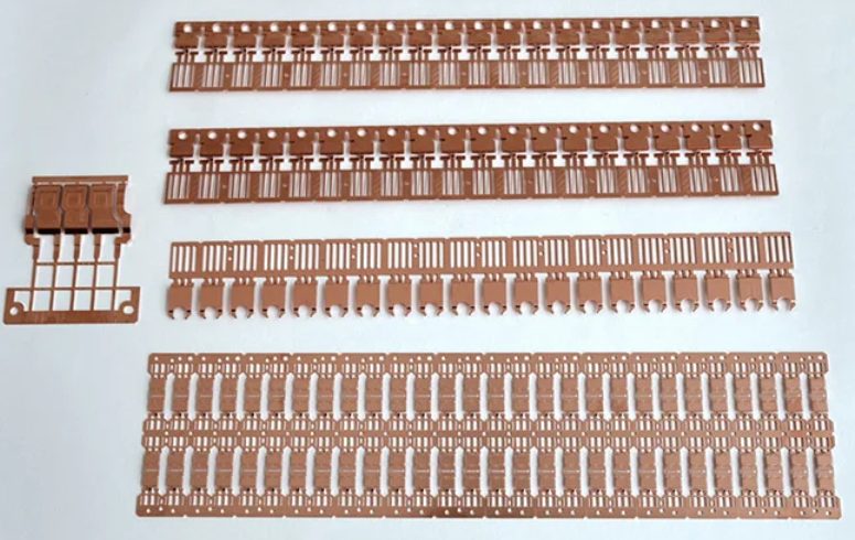
A Lead Frame is a metal framework used in semiconductor packaging to electrically connect the chip to external leads. Made from materials like copper or copper alloys, the Lead Frame serves as a structural base that provides electrical paths and mechanical support to the IC. Its design is critical in maintaining the integrity and performance of the chip throughout its lifecycle, making it an indispensable element in modern IC packaging technologies.
What is a Lead Frame in Lead Frames on Chip Package?
A Lead Frame is a crucial component in semiconductor packaging, particularly in Lead Frames on Chip Package, where it serves as the interface between the integrated circuit (IC) and the external electrical world. The Lead Frame is typically made from metal materials such as copper, copper alloys, or iron-nickel alloys, chosen for their excellent conductivity, strength, and thermal properties. It is used to connect the delicate semiconductor chip to the external circuits, ensuring efficient electrical transmission and providing the necessary mechanical support.
The structure of a Lead Frame consists of several key components:
- Frame: The frame acts as the structural base that holds the other components in place. It provides a foundation for the leads and the chip, ensuring stability and proper alignment within the package.
- Leads: The leads are metal pins or leads that extend from the frame to provide electrical contact between the semiconductor chip and the external circuitry. These leads allow signals to be transmitted to and from the IC once it is packaged.
- Metal Pins: These pins or leads are used to transfer electrical signals from the chip to the external environment. They are typically attached to the chip through wire bonding, which ensures a reliable electrical connection.
In Lead Frames on Chip Package, the design and material choice for the Lead Frame are critical to the overall performance, cost-efficiency, and reliability of the final product. The precise engineering of these components ensures that the IC is well-protected, while also allowing for high-performance operation in various applications.
How Does a Lead Frame Work in Lead Frames on Chip Package?
In Lead Frames on Chip Package, the Lead Frame plays a fundamental role in connecting the integrated circuit (IC) to the external environment. Its primary function is to facilitate both electrical and mechanical connections, ensuring the smooth operation of the semiconductor device once it’s packaged.
Connection Between Chip and Leads
The Lead Frame enables the connection between the semiconductor chip and the external leads, which are responsible for carrying electrical signals to and from the chip. Once the IC chip is placed onto the Lead Frame, the wire bonding process is typically used to make a secure connection between the chip’s bonding pads and the leads. The metal leads, which extend from the frame, serve as conductive pathways for the electrical signals that the chip processes.
These leads act as the interface between the chip’s internal circuitry and the external components it interacts with, such as other ICs or circuit boards. This connection is essential for the IC to communicate and function effectively in any electronic device, from smartphones to automobiles.
Electrical Connectivity and Mechanical Support
In addition to electrical connectivity, the Lead Frame provides crucial mechanical support during the packaging process. The metal frame holds the chip in place, preventing any movement or shifting that could disrupt the delicate wire bonds or damage the chip. This mechanical stability ensures that the chip remains securely attached to the package throughout its operational lifetime.
The Lead Frame also aids in thermal management. As the IC operates, it generates heat, and the Lead Frame helps to dissipate this heat away from the chip, preventing overheating and ensuring consistent performance. By providing a stable and conductive structure, the Lead Frame not only allows the electrical signals to flow but also ensures the IC’s longevity and reliability in Lead Frames on Chip Package applications.
The Lead Frame is an indispensable component in semiconductor packaging, combining electrical functionality with mechanical integrity, which is vital for the successful operation of ICs in modern electronics.
Comparing Lead Frame with Other Packaging Components in Lead Frames on Chip Package
In Lead Frames on Chip Package, it is important to understand how the Lead Frame compares to other packaging components like substrates and chip carriers. Each of these components plays a unique role in the overall function and performance of the semiconductor device, and knowing their differences helps highlight the advantages of using Lead Frames.
Lead Frame vs. Substrate
One of the main differences between a Lead Frame and a substrate lies in their functions, materials, and manufacturing processes.
-
Function:
- The Lead Frame primarily serves as the electrical and mechanical connection between the IC chip and the external circuitry, as well as providing support and thermal dissipation during packaging. It is generally used in Lead Frames on Chip Package for cost-effective and high-volume applications.
- A substrate, on the other hand, is a more complex platform that also provides electrical connections but tends to be used in more advanced or larger packaging solutions. Substrates often carry multi-layered circuitry and complex routing for interconnections, which can support higher pin counts and more intricate designs.
-
Materials:
- Lead Frames are typically made from materials like copper or copper alloys, which are known for their high electrical conductivity and thermal performance.
- Substrates are often made from materials like epoxy resin or ceramic, and feature layers of metal traces or conductive paths that help route the signals from the IC to external components. Substrates can be more expensive due to their multi-layer construction and ability to support more complex designs.
-
Manufacturing Process:
- The Lead Frame is typically manufactured using stamping or etching processes to create the frame and leads, followed by wire bonding to attach the chip to the leads. It is a simpler and more cost-effective process, making Lead Frames ideal for high-volume production.
- The substrate manufacturing process is more intricate and typically involves techniques like lamination and via-plating to create multiple layers of conductive paths. This process is generally slower and more expensive, making substrates suited for more complex and high-performance packaging.
Lead Frame vs. Chip Carrier
When comparing Lead Frames on Chip Package to Chip Carriers, there are also significant differences in terms of design and usage:
-
Design:
- Lead Frames are usually designed with a single, metal frame that connects the IC to external leads. The design is relatively simple, but highly effective for standard packages such as QFN (Quad Flat No-lead) or SMD (Surface Mount Device) packages.
- Chip Carriers, however, are typically more elaborate. They can come in various forms such as Ceramic Chip Carriers or Plastic Chip Carriers, and are often used for devices that require more robust thermal or electrical management. Chip carriers may have additional features like heat sinks, or even multiple layers for signal routing, making them more complex in design.
-
Usage:
- Lead Frames on Chip Package are commonly used in high-volume consumer electronics like mobile devices, automotive applications, and other relatively simple systems that require efficient and cost-effective packaging.
- Chip Carriers are more often used in applications that require higher performance and reliability, such as high-power devices, power ICs, or systems that need to withstand extreme environmental conditions. Chip carriers are also used in more advanced packaging technologies like BGA (Ball Grid Array), where the carrier provides both support and electrical connections.
While Lead Frames on Chip Package are ideal for cost-effective, high-volume packaging solutions, substrates and chip carriers offer more complex designs that support advanced performance and specialized applications. The choice between these components depends largely on the specific needs of the IC, its performance requirements, and the overall design of the final product.
Lead Frame Applications in Various Packaging Types in Lead Frames on Chip Package
In Lead Frames on Chip Package, the Lead Frame plays a critical role in enabling electrical connections and supporting the semiconductor chip across a variety of packaging types. Its versatility allows it to be used in a range of package forms, including QFN, DIP, SMD, BGA, and others. Each packaging type leverages the unique properties of the Lead Frame to meet the specific needs of the application, whether it’s for consumer electronics, automotive systems, or industrial devices.
QFN Packaging: How Lead Frames Are Used in QFN (Quad Flat No-lead) Packaging
The QFN (Quad Flat No-lead) package is one of the most popular surface-mount packaging options that utilizes Lead Frames on Chip Package. In QFN packaging, the Lead Frame is used to form the metal leads, which extend out from the sides of the package. These leads allow for electrical connections to be made to the external circuitry while providing a compact, low-profile design.
-
Connection via Leads: In QFN packages, the leads are not visible from the top of the package, as the leads are placed underneath the package itself. The Lead Frame in this design connects the IC to the external circuit by providing the necessary paths for the electrical signals. This is made possible by the wire-bonding process where fine wires connect the chip to the lead fingers on the frame.
-
Thermal Management: Another key advantage of Lead Frames on Chip Package in QFN is their ability to efficiently dissipate heat. The QFN package design typically incorporates an exposed die paddle that connects to the Lead Frame, which helps improve heat transfer and overall thermal performance. This is crucial for high-power applications, as it prevents overheating and ensures the longevity of the chip.
QFN packages are widely used in applications where space and cost are important considerations, including smartphones, automotive electronics, and consumer gadgets. The use of Lead Frames in QFN packaging offers both electrical and mechanical advantages while maintaining a compact form factor.
Other Packaging Types: Lead Frame Applications in DIP, SMD, BGA, and More
Beyond QFN, Lead Frames on Chip Package also play a significant role in various other packaging types, each serving different needs within the semiconductor industry.
-
DIP (Dual In-line Package): The DIP is one of the earliest and simplest forms of semiconductor packaging. Lead Frames are used in this package to provide the necessary leads, which extend from either side of the package for through-hole mounting onto a circuit board. Lead Frames on Chip Package in DIP applications are ideal for through-hole designs, often seen in legacy or low-volume applications, like industrial control systems or early consumer electronics.
-
SMD (Surface-Mount Device): In SMD packages, Lead Frames are used to form the leads that allow the IC to be mounted directly onto the surface of a PCB (Printed Circuit Board). This eliminates the need for through-holes, enabling a more compact and efficient design. The Lead Frame in SMD packages often provides a more reliable and cost-effective solution for smaller devices, such as resistors, capacitors, and microcontrollers in consumer electronics.
-
BGA (Ball Grid Array): In BGA packaging, Lead Frames on Chip Package help facilitate the connections between the IC and the PCB through an array of solder balls positioned on the underside of the package. Although BGA packages often use a different approach to connection, the Lead Frame still plays an integral role in the structure, especially when dealing with power BGAs or high-performance BGAs that require robust thermal and electrical performance. The Lead Frame here ensures that the internal connections are securely made and can handle the demands of high-speed, high-power applications.
-
Other Packaging Types: Beyond QFN, DIP, SMD, and BGA, Lead Frames are also used in various specialized packages such as LGA (Land Grid Array) and SIP (Single In-line Package). These packages leverage the Lead Frame for specific use cases, including automotive electronics, communication devices, and power systems.
Lead Frames on Chip Package offer wide applicability across different semiconductor packaging types. Whether it’s the compact design requirements of QFN, the versatility of DIP and SMD, or the high-performance demands of BGA, the Lead Frame ensures reliable electrical connections, mechanical stability, and effective heat dissipation, all of which contribute to the overall performance and durability of the packaged IC.
Manufacturing Process of Lead Frames in Lead Frames on Chip Package
The manufacturing of Lead Frames on Chip Package involves a highly precise and efficient process that transforms raw materials into a critical component of semiconductor packaging. From the selection of materials to the final production stage, the entire process is designed to ensure the reliability, performance, and cost-effectiveness of the Lead Frame. Understanding this process is essential for appreciating how Lead Frames contribute to the success of IC packaging.
Overview of Production Process: From Material Selection to the Final Product
The Lead Frame manufacturing process begins with the selection of high-quality materials, typically metals with excellent electrical conductivity and thermal performance. The most common materials used are copper, copper alloys, and iron-nickel alloys, as they provide the ideal balance of cost, conductivity, and mechanical strength. Copper, for example, is chosen for its superior electrical properties, making it an excellent choice for Lead Frames on Chip Package, which need to carry high-frequency electrical signals without significant losses.
Once the material is selected, the next step is to cut the material into thin sheets or strips that will be shaped into the final Lead Frame components. This stage often involves rolling or stamping processes to produce flat, thin pieces of metal that will form the frame, leads, and other parts of the Lead Frame structure.
The design for the Lead Frame is transferred to the material. This design typically includes specific patterns for the leads, frame, and metal pins, as well as features for wire bonding. The Lead Frame is then punched or stamped into its final shape using high-precision dies. This step requires very tight tolerances, as the dimensions of the leads and the frame must meet the specifications for efficient electrical performance and reliable mechanical connections.
After the stamping process, the Lead Frame undergoes additional steps such as cleaning, plating, and etching to enhance its durability and electrical performance. Finally, the Lead Frame is inspected for quality and consistency, ensuring that it meets all required standards before being ready for assembly in the Lead Frames on Chip Package.
Common Manufacturing Methods: Stamping, Etching, Heat Treatment, and More
Several key manufacturing methods are commonly used in the production of Lead Frames on Chip Package, each contributing to the efficiency, precision, and durability of the final product.
-
Stamping:
- Stamping is one of the most commonly used methods in Lead Frame production. This process involves using a stamping press and a die to cut and shape the metal sheet into the desired form. The stamping process allows for the high-volume production of Lead Frames with very consistent shapes, making it ideal for mass production in the semiconductor industry. Stamping can produce both the frame and leads in one step, ensuring precision and reducing manufacturing time.
-
Etching:
- Etching is often used to create more intricate designs or features on the Lead Frame, such as fine patterns for wire bonding or small features that help in connecting the leads to the chip. Chemical etching or laser etching is used to selectively remove material, leaving behind the desired patterns or traces. Etching is particularly important for producing the micro-level features required in high-performance Lead Frames on Chip Package.
-
Heat Treatment:
- After stamping or etching, heat treatment is frequently applied to the Lead Frame. This step is used to improve the mechanical properties of the metal, such as strength and hardness, ensuring that the Lead Frame can support the semiconductor chip securely and resist deformation during the assembly and packaging process. Heat treatment also helps improve the electrical properties by removing internal stresses within the metal and ensuring uniform conductivity across the Lead Frame.
-
Plating:
- Plating is another critical step, especially for improving the surface properties of the Lead Frame. Common plating methods include gold plating, nickel plating, or silver plating. These plating materials improve the corrosion resistance and help ensure that the Lead Frame remains reliable over the life of the IC. The plating also improves the bondability of the Lead Frame, which is crucial for the wire bonding process in Lead Frames on Chip Package.
-
Inspection and Testing:
- After the manufacturing processes, each Lead Frame undergoes thorough inspection and testing to ensure its quality. This includes visual inspections, dimensional measurements, and electrical testing to ensure the Lead Frame meets the required standards. Any Lead Frames that do not meet the quality criteria are discarded or reworked to maintain high production standards.
The Lead Frames on Chip Package manufacturing process is a combination of material selection, precision stamping, advanced etching techniques, and heat treatment, all of which come together to create a high-performance packaging solution for semiconductors. By using these methods, manufacturers can ensure the consistency, reliability, and functionality of Lead Frames in various semiconductor applications.
Material Selection for Lead Frames in Lead Frames on Chip Package
The material selection for Lead Frames on Chip Package is a critical factor that influences the performance, reliability, and cost of the final product. Since Lead Frames serve as the electrical pathway between the integrated circuit (IC) and external connections, the materials used must possess specific properties to ensure optimal functionality, durability, and efficiency in the semiconductor packaging process. The choice of materials also directly impacts the thermal performance, conductivity, and manufacturability of the Lead Frame.
Common Materials for Lead Frames
Several materials are commonly used in the manufacturing of Lead Frames on Chip Package, each offering a unique set of benefits suited to different application requirements. The most popular materials include:
-
Copper:
- Copper is the most widely used material for Lead Frames on Chip Package due to its excellent electrical conductivity, which is essential for transmitting signals between the IC and external circuits. Copper also has superior thermal conductivity, making it an excellent choice for heat dissipation. This is especially important in high-performance packages where the chip generates significant heat.
- Copper is relatively affordable, easy to manufacture, and offers a good balance of strength and flexibility, allowing it to be easily stamped or etched into intricate shapes.
-
Copper Alloys:
- Copper alloys, such as copper-phosphorus and copper-tin, are often used when a balance of electrical conductivity and mechanical strength is required. Alloys tend to have improved mechanical properties, including higher resistance to stress and deformation, which is beneficial in Lead Frames on Chip Package for ensuring long-term stability.
- These alloys are particularly useful in applications where the Lead Frame needs to resist fatigue or where enhanced thermal and electrical conductivity is required. Copper alloys are often used in more demanding applications like automotive electronics or industrial devices.
-
Iron-Nickel Alloys:
- Iron-nickel alloys, such as Kovar, are frequently used for applications requiring specific thermal expansion characteristics. These alloys have a coefficient of thermal expansion (CTE) that closely matches that of silicon, the primary material used for semiconductor chips. This makes them ideal for Lead Frames on Chip Package in high-reliability applications, such as space or military electronics, where thermal stability is critical.
- Iron-nickel alloys are also known for their resistance to corrosion and their mechanical strength, which provides both durability and reliability over the life cycle of the semiconductor device.
-
Stainless Steel:
- Stainless steel is sometimes used in Lead Frames on Chip Package when additional corrosion resistance and mechanical strength are required. While it is not as conductive as copper, it provides excellent durability in harsh environmental conditions and is often used for Lead Frames in applications such as automotive, industrial, and outdoor electronics.
Factors Affecting Material Choice
The selection of the right material for Lead Frames on Chip Package depends on several key factors, each contributing to the overall performance and manufacturing cost. These factors include:
-
Cost:
- The material cost plays a significant role in determining the overall price of the semiconductor package. Copper, while providing excellent conductivity and thermal properties, is typically more affordable than specialty materials like iron-nickel alloys or stainless steel. For high-volume, cost-sensitive applications such as consumer electronics, cost-effective materials like copper or copper alloys are often preferred.
- On the other hand, in applications where the performance and reliability of the IC are paramount (such as automotive, medical, or aerospace), more expensive materials may be chosen to ensure the semiconductor’s longevity and function.
-
Electrical Conductivity:
- The primary role of the Lead Frame is to carry electrical signals between the chip and external components. Therefore, electrical conductivity is one of the most important factors to consider when selecting materials. Copper has the highest electrical conductivity of any common material used in Lead Frames on Chip Package, making it the preferred choice for most applications. Copper alloys also provide good conductivity while offering enhanced mechanical properties.
-
Thermal Conductivity:
- As semiconductors generate heat during operation, the thermal conductivity of the material becomes crucial. A Lead Frame with high thermal conductivity helps dissipate heat away from the chip, preventing overheating and ensuring stable operation. Copper excels in this regard, which is why it is commonly used in power electronics and high-performance packages.
- Materials like iron-nickel alloys may be chosen in specific cases where thermal expansion matching with the silicon chip is needed to avoid stress from temperature fluctuations.
-
Mechanical Strength and Durability:
- The mechanical strength of the Lead Frame material determines its ability to withstand stress and strain during both the manufacturing process and the lifetime of the device. Materials like copper alloys and iron-nickel alloys offer enhanced strength and resistance to deformation, which is vital for high-reliability applications.
- Durability is also important in applications where the Lead Frame may be exposed to harsh environmental conditions, such as humidity, temperature extremes, or corrosive substances. Stainless steel and iron-nickel alloys are commonly used in these scenarios to ensure the Lead Frame performs over a longer period.
-
Corrosion Resistance:
- For applications exposed to moisture, chemicals, or extreme temperatures, the corrosion resistance of the Lead Frame material is a key factor. Iron-nickel alloys and stainless steel offer superior corrosion resistance compared to copper, making them ideal for specialized applications like automotive, aerospace, and industrial electronics.
-
Manufacturability:
- The ease with which the material can be processed also affects its selection. Copper is highly versatile, easy to stamp, etch, and plate, which makes it ideal for mass production. Materials that are more difficult to process, such as some alloys, may require additional steps or specialized equipment, which can increase manufacturing time and cost.
The material chosen for Lead Frames on Chip Package is influenced by a combination of factors, including electrical conductivity, thermal performance, mechanical strength, corrosion resistance, cost, and ease of manufacturing. By carefully selecting the right material based on these criteria, manufacturers can ensure that the Lead Frame meets the specific requirements of the application while delivering high performance and reliability in the final packaged IC.
Advantages and Challenges of Lead Frames in Lead Frames on Chip Package
Lead Frames on Chip Package are an essential part of the semiconductor packaging industry, offering numerous advantages that contribute to their widespread use. However, as with any technology, there are also challenges that need to be considered. Understanding both the benefits and the limitations of Lead Frames on Chip Package is crucial for optimizing their use in various applications.
Advantages of Lead Frames on Chip Package
-
Low Cost: One of the primary advantages of Lead Frames on Chip Package is their cost-effectiveness. Compared to other types of semiconductor packaging, such as wire bonding or advanced chip-on-board technologies, Lead Frames are relatively inexpensive to produce. The materials used (such as copper or copper alloys) are not only affordable but also widely available, which helps reduce overall production costs. Additionally, the automated manufacturing processes associated with Lead Frames on Chip Package contribute to their low cost by minimizing labor costs and improving production efficiency.
-
High Reliability: Lead Frames on Chip Package are known for their high reliability, particularly in standard applications. The metal frame provides excellent electrical and mechanical connections between the chip and external circuits. Their robust structure ensures that the connections remain stable and durable over time, even in demanding conditions. Lead Frames also contribute to the thermal management of the package, helping to dissipate heat generated by the semiconductor, which improves the reliability and longevity of the device.
-
Easy Automation in Production: The manufacturing process for Lead Frames on Chip Package is highly suited to automation, which enables high-volume production with consistent quality. Processes such as stamping, etching, plating, and heat treatment can be easily automated, reducing the potential for human error and improving efficiency. This capability makes Lead Frames ideal for large-scale production of semiconductor packages used in consumer electronics, automotive components, and industrial systems, where high reliability and cost efficiency are essential.
Challenges of Lead Frames on Chip Package
-
High Precision Requirements: One of the main challenges of Lead Frames on Chip Package is the high level of precision required during the manufacturing process. The intricate designs of the Lead Frame, especially for high-performance packages, demand tight tolerances to ensure proper alignment and functionality. Small variations in the dimensions of the leads, frame, or bonding pads can result in poor electrical connections or mechanical stability, leading to failure in the final package. Achieving such precision requires advanced manufacturing equipment and strict quality control, which can increase production time and cost, especially in complex or custom designs. As the semiconductor industry continues to demand smaller, faster, and more powerful devices, the precision requirements for Lead Frames on Chip Package become even more critical.
-
Limitations in Materials and Design: While Lead Frames on Chip Package are versatile and effective in many applications, there are limitations in terms of materials and design flexibility. The materials commonly used, such as copper and copper alloys, offer excellent electrical conductivity but may not be suitable for every application. For example, high-power devices or devices exposed to extreme environmental conditions may require more specialized materials like iron-nickel alloys or stainless steel, which can be more expensive or difficult to process. Furthermore, Lead Frames on Chip Package are less adaptable to certain advanced packaging technologies, such as three-dimensional (3D) packaging or chip-on-chip designs. These newer technologies require more complex interconnections and structures that traditional Lead Frames may not be able to support effectively. In such cases, alternatives like flip-chip packaging or ball grid array (BGA) packages may be better suited to the requirements.
Lead Frames on Chip Package offer a range of advantages, including low cost, high reliability, and the ability to be mass-produced with automation. However, they also come with challenges related to precision manufacturing and limitations in materials and design flexibility. By understanding both the strengths and weaknesses of Lead Frames on Chip Package, manufacturers can make informed decisions when selecting the appropriate packaging technology for their semiconductor applications.
Future Trends in Lead Frame Technology for Lead Frames on Chip Package
As the semiconductor industry continues to advance, Lead Frames on Chip Package are evolving to meet the growing demands for higher performance, smaller form factors, and increased reliability. Technological advancements in packaging, coupled with trends toward smarter and more compact designs, are driving the future of Lead Frames on Chip Package. These developments not only aim to address current industry challenges but also open up new opportunities for innovation in material selection, design, and manufacturing processes.
Advancements in Packaging: How Lead Frame Technology Evolves with the Development of the Semiconductor Industry
The semiconductor industry is progressing at an exponential rate, with ever-increasing demands for faster processing speeds, reduced power consumption, and higher density in electronic devices. As a result, Lead Frames on Chip Package must evolve to accommodate these changes.
One of the key advancements in packaging is the move toward advanced multi-chip packages. These packages often require more sophisticated Lead Frame designs that support multiple chips in a single package. The traditional Lead Frame must be adapted to support multiple connections, ensure optimal heat dissipation, and maintain signal integrity between different chips. This requires more precise manufacturing techniques and the use of advanced materials to maintain the performance of the package while still ensuring cost efficiency.
Lead Frames on Chip Package are increasingly being designed to meet the growing demand for high-performance computing (HPC) and 5G technologies. These applications require Lead Frames that can handle greater electrical loads and high-frequency signals, necessitating the use of high-conductivity materials and advanced heat management techniques. As such, future Lead Frames will likely integrate better thermal conductivity materials and offer enhanced mechanical strength to withstand the stresses generated by faster processing speeds and higher power outputs.
As semiconductor packaging continues to evolve, there is a shift toward system-in-package (SiP) and system-on-chip (SoC) technologies. These packages integrate multiple functions into a single package, making them more compact while maintaining performance. As part of these trends, Lead Frames on Chip Package will need to evolve to support these highly integrated devices, requiring more intricate designs, innovative layouts, and even hybrid materials to provide both electrical and mechanical connections.
Trends Towards Smart Packaging and Miniaturization: The Demand for Innovation in Materials, Design, and Manufacturing of Lead Frames on Chip Package
The trend toward miniaturization in electronic devices is another driving force behind the future of Lead Frames on Chip Package. As electronic devices become smaller and more powerful, packaging technologies must also adapt. Lead Frames on Chip Package are required to shrink in size while maintaining high reliability and performance. This trend presents several challenges for material selection and design.
To support this miniaturization, Lead Frames on Chip Package will likely incorporate new materials that can offer improved performance at smaller scales. Advanced copper alloys, for example, may be used to improve electrical conductivity while reducing the size of the Lead Frame. Additionally, there is a growing interest in nanomaterials and composite materials that could further reduce the size of the Lead Frame without compromising its mechanical strength or electrical properties.
There is a noticeable shift toward smart packaging technologies that can monitor the health and performance of the device. For example, Lead Frames on Chip Package could be integrated with sensors that monitor temperature, humidity, or other environmental factors, enabling predictive maintenance and improving the overall reliability of the semiconductor package. These smart features could be especially valuable in industries such as automotive electronics, where failure is not an option, and in IoT (Internet of Things) devices, where devices are expected to function in diverse and often harsh environments.
3D packaging technologies are gaining traction as a means to achieve even greater miniaturization. By stacking chips vertically, these technologies can dramatically reduce the footprint of the device while increasing functionality. Lead Frames on Chip Package will need to accommodate this trend by incorporating more flexible designs that allow for the vertical integration of multiple chips. This could lead to the development of multi-layer Lead Frames or Lead Frames with integrated vertical interconnects, enabling the efficient transfer of signals between stacked chips.
The manufacturing processes for Lead Frames on Chip Package are also likely to undergo significant advancements. Additive manufacturing, or 3D printing, holds the potential to revolutionize how Lead Frames are produced. This technique allows for the precise placement of materials in complex geometries, which could enable the creation of highly customized Lead Frames that meet the specific needs of emerging packaging technologies. 3D printing could also help to reduce waste and lower production costs by using only the necessary material for each Lead Frame.
The future of Lead Frames on Chip Package is closely tied to the ongoing evolution of semiconductor technology. As the industry pushes for faster, smaller, and more efficient electronic devices, Lead Frames will need to adapt by incorporating advanced materials, innovative designs, and new manufacturing processes. The trends toward smart packaging, miniaturization, and multi-chip integration will continue to shape the development of Lead Frames on Chip Package, ensuring their crucial role in the future of semiconductor packaging.
Contact Us
FQAs Abut Lead Frames on Chip Package
What is a lead frame in semiconductor?
A lead frame is a metal structure used in semiconductor packaging to provide electrical connections between the chip and the external circuits. It typically consists of a metal frame, leads, and pins, all of which facilitate the physical and electrical connection of the integrated circuit (IC) to its external environment.
What does a lead frame do?
A lead frame serves two primary functions: it provides a mechanical structure that holds the chip in place within the package, and it establishes electrical connections between the chip’s bond pads and the external leads, allowing communication with the outside world. Additionally, it aids in heat dissipation during the operation of the semiconductor device.
What is meant by lead frame?
A lead frame refers to the metal base used in semiconductor packaging, which is responsible for supporting the integrated circuit (IC) and providing the necessary electrical connections through its leads and pins. It is a crucial part of the package that enables the chip to function within an electronic device by connecting it to the broader circuit board.
What is the difference between lead frame and substrate?
The lead frame and the substrate are both essential components in semiconductor packaging, but they serve different roles. A lead frame is a metal structure that connects the IC to external circuits, providing mechanical support and electrical pathways through its leads and pins. On the other hand, a substrate is typically a non-metallic material (often made of epoxy or ceramic) that provides the foundation for the IC, supporting the chip and its electrical connections. The substrate also serves to distribute electrical signals and provide additional heat dissipation. While the lead frame is metal and focuses on connectivity, the substrate is often insulating and aids in the stability and signal management of the package.

