
Essential Components: IC Package Substrates Explained
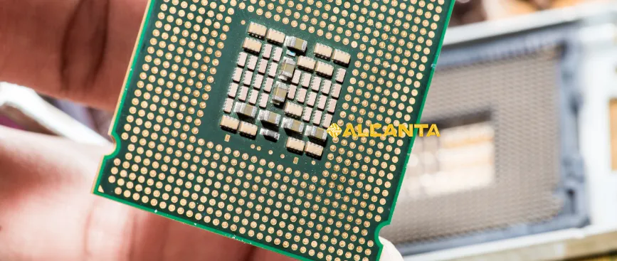
IC Package Substrate refers to a crucial component in integrated circuit (IC) packaging, providing a physical and electrical interface between the IC chip and the PCB. Its primary role is to facilitate electrical connections, thermal management, and structural support within a compact form factor. The substrate’s significance lies in optimizing signal integrity, reducing electrical noise, enhancing thermal dissipation efficiency, and ensuring reliability under varying operating conditions. As IC technologies advance, the substrate’s role becomes increasingly vital in meeting demands for higher performance, miniaturization, and reliability in modern electronic devices. Thus, understanding and innovating in IC Package Substrate design and materials are pivotal for advancing semiconductor packaging capabilities.
Types of IC Package Substrate
Coreless Substrate
Definition and Characteristics:
Coreless Substrate refers to a type of substrate that lacks a traditional solid core typically found in conventional substrates. Instead, it utilizes a thin dielectric layer with embedded circuit traces, allowing for a more compact and lightweight design. This design minimizes the overall thickness of the package, enhancing thermal management and electrical performance.
Applications and Advantages:
Coreless Substrates are often used in applications where size, weight, and electrical performance are critical factors. They are favored in high-frequency applications such as RF (Radio Frequency) modules, wireless communication devices, and high-speed data transfer systems. Advantages include reduced parasitic capacitance, improved signal integrity, and enhanced thermal dissipation due to their efficient heat transfer capabilities.
Embedded Trace Substrate
Definition and Characteristics:
Embedded Trace Substrate features embedded conductive traces within the substrate material itself, eliminating the need for separate wiring layers. This design integrates signal paths directly into the substrate, reducing signal loss and electromagnetic interference (EMI). Embedded traces are typically made using specialized dielectric materials with high electrical performance and thermal conductivity.
Overview of Design and Manufacturing Process:
The design of Embedded Trace Substrates involves intricate layout planning to embed traces within the substrate material during manufacturing. This process includes laser drilling or etching techniques to create pathways for signal routing. Advanced manufacturing technologies ensure precise alignment and insulation of embedded traces, maintaining high reliability and electrical performance in demanding applications such as high-speed digital circuits and compact consumer electronics.
These types of IC Package Substrates demonstrate specialized designs and manufacturing processes tailored to optimize electrical performance, thermal management, and reliability in various semiconductor packaging applications.
Materials Used in IC Package Substrate
Commonly Used Materials and Their Properties
In IC Package Substrates, various materials are chosen based on their electrical, thermal, mechanical, and cost properties:
– High Temperature Co-Fired Ceramic (HTCC): HTCC substrates are known for their excellent thermal conductivity, high mechanical strength, and reliability at elevated temperatures. They are ideal for applications requiring robust thermal management and durability.
– Low Temperature Co-Fired Ceramic (LTCC): LTCC substrates offer similar properties to HTCC but can be fired at lower temperatures, making them suitable for integrating passive components like resistors, capacitors, and inductors directly into the substrate.
– Polyimide (PI): PI substrates provide flexibility, lightweight construction, and good electrical insulation properties. They are used in applications requiring high-density interconnects and flexibility, such as flexible circuits and wearables.
– Traditional Substrates like FR-4: FR-4 substrates are cost-effective and widely used in standard PCB applications due to their good mechanical properties, ease of fabrication, and compatibility with lead-free soldering processes.
Comparative Suitability of Different Materials
Choosing the right substrate material depends on specific application requirements:
– Electrical Performance: HTCC and LTCC offer superior electrical performance with low dielectric loss and high-frequency capability compared to organic materials like PI and FR-4.
– Thermal Management: Ceramic substrates (HTCC/LTCC) excel in thermal conductivity, crucial for dissipating heat from high-power components, whereas PI and FR-4 have lower thermal conductivity but sufficient for many standard applications.
– Mechanical Strength: Ceramic substrates provide high mechanical strength and dimensional stability, whereas PI offers flexibility and bendability.
High Temperature Co-Fired Ceramic (HTCC) and Low Temperature Co-Fired Ceramic (LTCC)
– HTCC: Suited for high-power applications, HTCC substrates withstand temperatures above 300°C and offer excellent thermal conductivity and mechanical strength.
– LTCC: Used for integrated passive devices, LTCC substrates fire at lower temperatures (typically below 1000°C) and allow for embedding resistors, capacitors, and inductors within the substrate layers.
Polyimide (PI) and Traditional Substrates like FR-4
– PI: Offers flexibility and excellent electrical insulation, suitable for flexible circuits and applications requiring conformal designs.
– FR-4: Cost-effective and versatile, FR-4 substrates are widely used in consumer electronics, telecommunications, and industrial applications due to their balance of performance and affordability.
These material choices illustrate the diversity and specialized characteristics required to meet the varied demands of modern IC packaging, ensuring optimal performance, reliability, and cost-efficiency across different applications.
Manufacturing Process of IC Package Substrate
Overview of Typical Manufacturing Processes
The manufacturing of IC Package Substrates involves several critical processes to achieve precise electrical and mechanical properties:
1. Substrate Preparation:
– Raw material selection based on application requirements (e.g., ceramic, polyimide).
– Material processing such as mixing, milling, and forming into sheets or tapes.
2. Layer Formation:
– Deposition or casting of substrate layers with controlled thickness and material composition.
– For ceramic substrates (HTCC/LTCC), layers are often screen-printed with conductive pastes or embedded with passive components.
3. Circuit Patterning:
– Photolithography or laser ablation to define circuit patterns and vias for interconnects.
– Metal deposition (e.g., copper, gold) through plating or sputtering to form conductive traces and pads.
4. Stacking and Lamination:
– Layer stacking to build up the substrate structure with alternating conductive and insulating layers.
– Lamination under controlled temperature and pressure to bond layers and ensure interlayer connectivity.
5. Post-Processing:
– Cutting, routing, and drilling to create final substrate dimensions and accommodate specific component placements.
– Surface finishing such as solder mask application and surface treatment for solderability and protection.
Key Steps and Technological Highlights
– Precision Control: Advanced manufacturing technologies ensure precise layer thickness, alignment of circuit patterns, and vias, critical for high-density interconnects and signal integrity.
– Embedding Components: Specialized techniques allow for embedding passive components directly into substrate layers, enhancing miniaturization and electrical performance in integrated designs.
– High-Temperature Processes: For ceramic substrates (HTCC/LTCC), firing processes at controlled temperatures ensure proper sintering of ceramic materials and integration of embedded components.
– Environmental Considerations: Manufacturing processes are optimized for environmental factors such as temperature, humidity, and clean room requirements to maintain consistent quality and reliability.
– Quality Assurance: Rigorous testing protocols including electrical testing, thermal cycling, and mechanical stress testing ensure substrates meet performance specifications and reliability standards.
The complexity and precision of these manufacturing processes underscore the importance of technological innovation and expertise in producing IC Package Substrates that meet the stringent demands of modern semiconductor packaging applications.
Applications of IC Package Substrate in IC Packaging
Case Studies of Applications in Different Types of Packaging Technologies
IC Package Substrates play a pivotal role across various packaging technologies, each tailored to specific application requirements:
1. Ball Grid Array (BGA) Packages:
– Application: High-performance CPUs and GPUs in computing devices.
– Substrate Role: Provides high-density interconnects and efficient heat dissipation crucial for processors operating at high speeds and power levels.
2. Quad Flat Packages (QFP):
– Application: Consumer electronics such as microcontrollers and memory modules.
– Substrate Role: Supports multiple pins for signal transmission and power delivery while maintaining compact dimensions suitable for handheld devices.
3. System in Package (SiP) Integration:
– Application: Mobile devices integrating multiple functions (e.g., RF, memory, sensors).
– Substrate Role: Facilitates miniaturization by integrating diverse components on a single substrate, enhancing performance and reducing PCB footprint.
Examples of Applications in Various Packaging Techniques
IC Package Substrates are utilized in diverse packaging techniques to meet specific performance and design criteria:
– 3D Packaging: IC Package Substrates enable vertical stacking of dies, enhancing performance density and reducing interconnect length for faster signal propagation in applications like high-performance computing and data centers.
– Flip Chip Technology: Substrates support direct die attachment and interconnects using solder bumps, reducing signal path lengths and improving electrical performance in applications requiring high-speed data transmission and low latency.
– Wafer Level Packaging (WLP): Utilizing advanced IC Package Substrates allows for packaging at the wafer level, reducing costs and enhancing manufacturing efficiency for applications in consumer electronics and IoT devices.
– Photonics Integration: In emerging applications such as optical interconnects and LiDAR systems, IC Package Substrates enable integration of photonic components for high-speed data transmission and sensing applications.
These examples highlight the versatility and critical role of IC Package Substrates in enabling advanced packaging technologies to meet the evolving demands of modern electronic devices across various industries and applications.
Future Trends in IC Package Substrate
Technological Innovations and Market-Driven Demands
Technological advancements and evolving market demands are driving innovations in IC Package Substrates:
– Advanced Materials: Continued development of materials with enhanced electrical conductivity, thermal management properties, and reliability to support higher frequencies and power densities.
– Miniaturization: Demand for smaller, thinner, and more integrated packages to support compact consumer electronics, IoT devices, and automotive applications.
– Integration of Passive Components: Increasing integration of passive components (e.g., resistors, capacitors, inductors) directly into substrates to reduce footprint and enhance performance in high-frequency applications.
– High-Speed and High-Frequency Applications: Growing requirements for substrates capable of supporting higher data rates and frequencies in 5G communications, artificial intelligence (AI), and autonomous vehicles.
Predictions for Future Developments and Trends Over the Coming Years
Looking ahead, several trends are expected to shape the future of IC Package Substrates:
– Emergence of 3D Packaging: Expanded adoption of 3D packaging techniques using advanced substrates to achieve greater performance density and improved thermal management.
– Flexible and Stretchable Substrates: Development of flexible substrates using materials like polyimide and elastomers to enable conformal designs for wearable electronics and biomedical applications.
– Environmental Sustainability: Increasing focus on eco-friendly manufacturing processes and materials, addressing concerns over electronic waste and energy efficiency.
– Integration with Emerging Technologies: Integration of substrates with emerging technologies such as photonics and quantum computing to meet the demands of next-generation computing and communication systems.
– Industry 4.0 and Smart Manufacturing: Adoption of smart manufacturing practices integrating IoT and AI to enhance substrate fabrication processes, improve quality control, and reduce time-to-market.
These trends indicate a dynamic future for IC Package Substrates, driven by technological advancements, market demands for higher performance and miniaturization, and integration with cutting-edge technologies across various industries.
FAQs about ic package substrate
In IC (Integrated Circuit) packaging, the substrate refers to a base layer or material upon which the integrated circuit is mounted. It provides a foundation for the IC components and facilitates electrical connections between the IC and external circuitry.
A semiconductor package substrate is a specialized substrate used in the packaging of semiconductor devices, such as integrated circuits (ICs) and microchips. It typically consists of materials with good electrical conductivity and thermal properties to ensure efficient performance and reliability of the semiconductor device.
Various materials are used for IC packaging substrates, depending on the specific requirements of the semiconductor device. Common materials include ceramics (such as alumina and aluminum nitride), organic materials (such as epoxy resins and polyimides), and metal alloys (such as copper and copper alloys). These materials are chosen based on factors like thermal conductivity, electrical insulation, mechanical strength, and cost-effectiveness.
The substrate of ICs refers to the base layer or material on which the integrated circuit components are fabricated and mounted. It plays a crucial role in providing mechanical support, electrical connections, and thermal management for the IC. The substrate also contributes to the overall performance and reliability of the integrated circuit.

