
The Vital Functions of Substrate IC in Electronics
Integrated circuits (ICs) are the fundamental building blocks of modern electronic devices, enabling the compact integration of millions to billions of electronic components on a single semiconductor substrate. Their significance in technology spans from everyday consumer electronics to complex industrial applications, driving advancements in computing, telecommunications, and beyond.
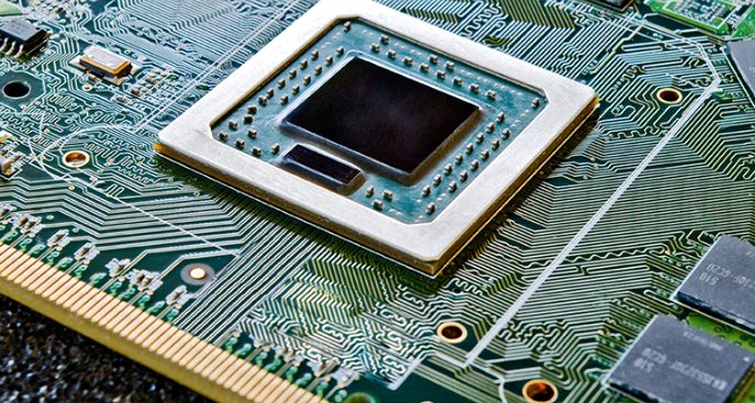
Central to the manufacturing of ICs is the role of IC substrates, which serve as the physical foundation for mounting and interconnecting semiconductor devices within the integrated circuit. These substrates not only support the delicate semiconductor components but also facilitate electrical connections, heat dissipation, and signal integrity crucial for the functionality and performance of ICs. Understanding the composition, manufacturing processes, and technological advancements in IC substrates is essential for grasping their pivotal role in advancing electronic innovations globally.
What is an IC Substrate?
Definition of IC Substrate
An IC substrate is a specialized base material used in the construction of integrated circuits (ICs). It serves as a platform for mounting and interconnecting various semiconductor devices that comprise an IC. Typically made from materials like ceramics, metals, or laminates, IC substrates provide structural support and facilitate electrical connections between the semiconductor components and the rest of the circuitry.
Main Functions and Uses of IC Substrates
IC substrates play several critical roles in the manufacturing and performance of integrated circuits:
- Mechanical Support: IC substrates provide a sturdy base for semiconductor devices, ensuring they are securely mounted and protected from physical damage.
- Electrical Interconnection: They facilitate the routing of electrical signals between different components of the IC, ensuring proper functioning of the circuit.
- Heat Dissipation: IC substrates help in dissipating heat generated during the operation of the IC, thereby maintaining optimal operating temperatures and preventing overheating.
- Signal Integrity: They contribute to maintaining signal integrity by minimizing electrical noise and interference, crucial for reliable operation in high-frequency applications.
- Miniaturization: IC substrates enable the compact design of ICs by allowing components to be densely packed, thereby enhancing performance and reducing overall size.
Understanding these functions underscores the importance of IC substrates in modern electronics, where efficiency, reliability, and miniaturization are paramount considerations.
Materials of IC Substrates
What materials are IC substrates usually made of?
IC substrates are typically fabricated from various materials, each chosen based on specific performance requirements and manufacturing processes:
- Ceramics:
- Materials: Alumina (Al2O3) and aluminum nitride (AlN) are common ceramics used for their excellent thermal conductivity and mechanical strength.
- Advantages: Superior heat dissipation, high electrical insulation, and compatibility with high-frequency applications.
- Disadvantages: Brittle nature, higher cost compared to other materials.
- Metals:
- Materials: Copper and copper alloys are widely used due to their good electrical conductivity and manufacturability.
- Advantages: Excellent electrical and thermal conductivity, cost-effective, and suitable for large-scale production.
- Disadvantages: Susceptible to corrosion, may require surface treatment for improved performance.
- Laminates:
- Materials: Epoxy resin or polyimide-based laminates (e.g., FR-4) are common in PCB-like substrates.
- Advantages: Cost-effective, flexible, and readily available for standard PCB manufacturing processes.
- Disadvantages: Lower thermal conductivity compared to ceramics and metals, limiting their use in high-power applications.
- Semiconductor Grade Silicon:
- Materials: Silicon substrates are used in specialized applications, such as MEMS (Micro-Electro-Mechanical Systems) and certain types of ICs.
- Advantages: Compatible with semiconductor fabrication processes, allowing integration of active devices and sensors.
- Disadvantages: Expensive, limited to specific applications requiring semiconductor-grade purity.
Advantages and disadvantages of different materials:
- Ceramics:
- Advantages: High thermal conductivity, excellent mechanical strength.
- Disadvantages: Brittle, higher cost.
- Metals:
- Advantages: Good electrical and thermal conductivity, cost-effective.
- Disadvantages: Susceptible to corrosion.
- Laminates:
- Advantages: Cost-effective, flexible, suitable for standard PCB processes.
- Disadvantages: Lower thermal conductivity.
- Semiconductor Grade Silicon:
- Advantages: Integration with semiconductor processes.
- Disadvantages: Expensive, limited applications.
Each material choice involves trade-offs between electrical performance, thermal management, cost, and manufacturability, highlighting the importance of selecting the right substrate material based on specific IC design requirements and application needs.
Differences Between IC Substrate and PCB
Define PCB (Printed Circuit Board)
A Printed Circuit Board (PCB) is a flat board made of non-conductive material (typically fiberglass reinforced epoxy laminate) with conductive pathways etched or printed onto it to connect various electronic components mounted on the board. PCBs are fundamental in electronic devices for providing mechanical support and electrical connections between components.
Compare the Structure and Functions of IC Substrates and PCBs
Structure:
- IC Substrate: Typically made from materials like ceramics or laminates, IC substrates are designed to support and interconnect semiconductor devices within an integrated circuit.
- PCB: Composed of layers of non-conductive substrate (core) sandwiched between layers of copper foil (traces) and laminated together. PCBs provide a platform for mounting and interconnecting a wide range of electronic components.
Functions:
- IC Substrate: Primarily focuses on providing a stable base for semiconductor devices, facilitating electrical connections, heat dissipation, and signal integrity crucial for IC operation.
- PCB: Acts as a backbone for electronic circuits, enabling the routing of signals between components, power distribution, and mechanical support for components like resistors, capacitors, and integrated circuits.
Guidelines for Choosing Between IC Substrates and PCBs in Specific Applications
- Complexity and Integration:
- IC Substrates: Ideal for applications requiring high integration density and specific performance characteristics like thermal management and signal integrity (e.g., microprocessors, high-frequency ICs).
- PCBs: Suitable for general-purpose applications where flexibility in component placement and cost-effectiveness are prioritized (e.g., consumer electronics, automotive electronics).
- Performance Requirements:
- IC Substrates: Chosen for applications demanding high-speed signal transmission, minimal noise interference, and efficient heat dissipation.
- PCBs: Used in applications where moderate signal integrity and thermal management suffice, with emphasis on cost-efficiency and manufacturability.
- Cost and Manufacturing Considerations:
- IC Substrates: Typically more expensive due to specialized materials and manufacturing processes, suitable for high-performance and niche applications.
- PCBs: Economical choice for mass production, leveraging standardized manufacturing processes and materials suitable for a wide range of electronic devices.
Choosing between IC substrates and PCBs involves evaluating specific design requirements, performance expectations, and cost considerations. The decision impacts the overall functionality, reliability, and cost-effectiveness of electronic systems, emphasizing the need for careful consideration based on application-specific needs.
IC Substrate Manufacturing Process
Detailed Manufacturing Steps
The manufacturing of IC substrates involves several intricate steps to ensure the precise fabrication of substrates that meet stringent performance and reliability standards:
- Substrate Preparation:
- Material Selection: Choose appropriate substrate material (e.g., ceramics, metals, laminates) based on design requirements.
- Cleaning and Preparation: Clean and prepare the substrate surface to ensure optimal adhesion and cleanliness.
- Lamination or Deposition:
- Layer Deposition: For multilayer substrates, deposit conductive and insulating layers using techniques like physical vapor deposition (PVD) or chemical vapor deposition (CVD).
- Lamination: For laminated substrates, bond layers of substrate material together using heat and pressure.
- Pattern Formation:
- Photolithography: Define the circuit pattern using photolithography, involving the use of photoresist, UV light exposure, and etching to remove unwanted material.
- Metalization: Deposit metal layers (typically copper) onto the substrate surface to form conductive pathways using techniques like electroplating or sputtering.
- Etching and Surface Treatment:
- Etching: Remove excess metal and substrate material not protected by photoresist using chemical etchants.
- Surface Treatment: Apply surface treatments such as chemical cleaning or plasma treatment to enhance adhesion and surface properties.
- Quality Control and Testing:
- Dimensional Inspection: Measure critical dimensions and features to ensure adherence to design specifications.
- Electrical Testing: Verify electrical connectivity and insulation integrity of conductive pathways.
- Thermal Testing: Assess thermal conductivity and heat dissipation properties.
- Visual Inspection: Inspect for defects such as cracks, delamination, or uneven metallization.
Technologies and Equipment Involved
- Photolithography Systems: Used for defining circuit patterns on substrates.
- Deposition Equipment: Includes PVD and CVD systems for depositing metal and insulating layers.
- Etching Equipment: Chemical etchants and plasma etching systems for removing unwanted material.
- Lamination Machines: Equipment for bonding multiple substrate layers together.
- Testing and Inspection Tools: Includes coordinate measuring machines (CMM), electrical testers, thermal analyzers, and optical inspection systems.
Quality Control and Inspection Methods
- Statistical Process Control (SPC): Monitor and control process variables to ensure consistent quality.
- Automated Optical Inspection (AOI): Use optical systems to inspect circuit patterns and detect defects.
- X-ray Inspection: Non-destructive testing to examine internal structures and detect hidden defects.
- Microscopic Examination: Visual inspection using high-resolution microscopy to identify minute defects.
- Functional Testing: Assess the substrate’s performance under operating conditions to validate functionality and reliability.
By meticulously following these manufacturing steps and employing advanced technologies for quality control and inspection, IC substrate manufacturers ensure the production of substrates that meet the demanding requirements of modern integrated circuits.
Major IC Substrate Manufacturers
Companies like AT&S and Other Well-Known Manufacturers
AT&S (Austria Technologie & Systemtechnik AG):
- Overview: AT&S is a leading manufacturer of high-end IC substrates, focusing on advanced packaging solutions for various semiconductor applications.
- Technological Advantages: Known for their expertise in high-density interconnect (HDI) substrates, which support miniaturization and high-speed performance in ICs.
- Market Position: AT&S holds a significant market share in the global IC substrate industry, catering to diverse sectors including telecommunications, automotive electronics, and consumer electronics.
Other Well-Known Manufacturers
Taiwan Semiconductor Manufacturing Company (TSMC):
- Overview: TSMC is renowned for its semiconductor foundry services but also manufactures advanced IC substrates.
- Technological Advantages: Offers innovative packaging solutions such as fan-out wafer-level packaging (FO-WLP) and system-in-package (SiP) technologies.
- Market Position: TSMC’s extensive capabilities in both semiconductor manufacturing and IC substrate production place it among the top players globally.
Samsung Electro-Mechanics (SEMCO):
- Overview: SEMCO is a subsidiary of Samsung Group specializing in various electronic components, including IC substrates.
- Technological Advantages: Focuses on high-performance substrates for mobile devices, leveraging Samsung’s semiconductor expertise.
- Market Position: Strong presence in the mobile electronics sector and expanding into other high-growth areas of electronics packaging.
Kyocera Corporation:
- Overview: Kyocera manufactures a range of electronic components, including ceramic IC substrates.
- Technological Advantages: Offers ceramic substrates with excellent thermal management properties and reliability for demanding applications.
- Market Position: Well-established in the automotive, industrial, and telecommunications sectors due to their durable and high-performance substrates.
Market Position and Technological Advantages of These Companies
These major IC substrate manufacturers differentiate themselves through:
- Technological Innovation: Continuous development of advanced packaging solutions like HDI, FO-WLP, and SiP technologies to meet evolving market demands.
- Quality and Reliability: Ensuring high standards in manufacturing processes to deliver substrates with superior performance, reliability, and durability.
- Global Reach: Extensive manufacturing facilities and distribution networks worldwide, supporting diverse customer needs across different industries.
- Strategic Partnerships: Collaborations with leading semiconductor companies to co-develop next-generation packaging solutions.
By leveraging these strengths, companies like AT&S, TSMC, SEMCO, and Kyocera maintain leadership positions in the competitive IC substrate market, driving innovation and enabling advancements in semiconductor packaging technologies.
Emerging Technology: Substrate-like PCB
What is Substrate-like PCB?
Substrate-like PCB (SLP) is an advanced type of printed circuit board that combines the high-density interconnect (HDI) capabilities of IC substrates with the traditional manufacturing processes of PCBs. It offers a middle ground between conventional PCBs and IC substrates, providing enhanced performance and design flexibility.
Innovations and Potential Applications of this Technology
Innovations:
- High-Density Interconnect (HDI): SLPs incorporate multiple layers of thin dielectric materials and fine-pitch copper wiring, allowing for densely packed components and signal traces.
- Miniaturization: Enables the design of smaller and lighter electronic devices by reducing the footprint and thickness of the PCB while maintaining functionality.
- Embedded Components: Integration of passive and active components within the substrate layers, optimizing space utilization and improving electrical performance.
- Advanced Materials: Use of advanced materials with improved thermal conductivity and signal integrity, enhancing overall reliability and performance.
Potential Applications:
- Mobile Devices: SLPs are ideal for smartphones, tablets, and wearables where compact size and high performance are critical.
- Automotive Electronics: Used in vehicle infotainment systems, navigation devices, and advanced driver-assistance systems (ADAS) due to their reliability and durability.
- IoT Devices: Suitable for IoT applications requiring small form factors and efficient power management.
- High-Frequency Applications: SLPs support high-speed data transmission and RF applications, making them suitable for telecommunications and networking equipment.
- Consumer Electronics: Applied in laptops, cameras, and gaming consoles where space-saving and enhanced functionality are desired.
By leveraging the advantages of both IC substrates and traditional PCBs, substrate-like PCBs represent a significant advancement in electronic packaging technology. Their ability to integrate complex functionalities into compact designs while maintaining high reliability positions them as a preferred choice for next-generation electronic devices across various industries.
Introduction to ABF Substrate
Definition and Applications of ABF Substrate
Definition: Anisotropic Conductive Film (ABF) substrate is a type of polyimide-based flexible circuit board known for its exceptional electrical and thermal properties. ABF substrates are used primarily in high-frequency and high-performance applications where reliability and signal integrity are critical.
Applications:
- High-Frequency ICs: ABF substrates are widely used in RF (Radio Frequency) and microwave ICs due to their low dielectric constant and loss tangent, which minimize signal loss and interference.
- Wireless Communication: Commonly found in wireless communication devices such as mobile phones, WiFi routers, and satellite communication systems.
- Data Transmission: Used in high-speed data transmission applications like servers, data centers, and optical communication equipment.
- Automotive Electronics: Applied in automotive radar systems, navigation systems, and ADAS (Advanced Driver Assistance Systems) due to their robustness and reliability.
Importance in High-Performance ICs
ABF substrates play a crucial role in enhancing the performance of high-speed and high-frequency ICs:
- Signal Integrity: ABF substrates offer excellent signal integrity by minimizing signal loss, cross-talk, and electromagnetic interference (EMI), crucial for maintaining data accuracy and reliability in high-speed circuits.
- Thermal Management: Their ability to dissipate heat efficiently helps in maintaining optimal operating temperatures, ensuring stable performance of ICs under varying environmental conditions.
- Miniaturization: ABF substrates support the design of compact and lightweight electronic devices by allowing for densely packed components and intricate circuit designs.
- Reliability: Known for their mechanical flexibility and durability, ABF substrates enhance the overall reliability and longevity of electronic systems, making them suitable for demanding applications in aerospace, telecommunications, and industrial sectors.
ABF substrates are pivotal in advancing the capabilities of high-performance ICs, offering superior electrical characteristics, thermal management, and reliability essential for modern electronic applications across diverse industries.
Role of IC Substrates in Chip Packaging
How IC Substrates are Used in Chip Packaging
IC substrates play a critical role in chip packaging by providing a robust platform for mounting and interconnecting semiconductor devices. The process involves several key functions:
- Mounting and Interconnection: IC substrates serve as a structural foundation for attaching semiconductor chips (integrated circuits). They provide solder pads or bump pads for connecting the chip’s input/output (I/O) pads to the rest of the circuitry.
- Signal Routing: Electrical pathways within the substrate route signals between the chip and other components on the printed circuit board (PCB) or within the system. These pathways are designed to minimize signal loss and interference, ensuring reliable communication between components.
- Heat Dissipation: IC substrates facilitate the dissipation of heat generated by the semiconductor devices during operation. Thermal vias, conductive layers, and thermal management materials are integrated into the substrate design to efficiently transfer heat away from the chip, maintaining optimal operating temperatures and prolonging component lifespan.
- Mechanical Support: IC substrates provide mechanical support to the semiconductor chip, protecting it from physical stress, shock, and vibration. This support is crucial for maintaining the structural integrity of the chip package in various environmental conditions.
Impact on Performance and Reliability
The use of high-quality IC substrates in chip packaging significantly impacts both the performance and reliability of electronic devices:
- Performance: IC substrates with advanced design features, such as high-density interconnects (HDI) and low-loss materials, enhance signal transmission speed and integrity. This capability is vital for applications requiring high-speed data processing and communication, such as telecommunications equipment, servers, and consumer electronics.
- Reliability: By optimizing thermal management and ensuring robust mechanical support, IC substrates contribute to the overall reliability and longevity of semiconductor devices. Reliable operation is crucial in critical applications like automotive electronics, aerospace systems, and medical devices where downtime or failure can have serious consequences.
- Miniaturization: The compact design enabled by IC substrates allows for smaller and lighter electronic devices without compromising performance. This miniaturization trend is essential for advancements in portable electronics, wearable devices, and IoT applications.
IC substrates play a pivotal role in chip packaging by providing essential functions such as mounting, interconnection, signal routing, heat dissipation, and mechanical support. Their impact on performance enhancement, reliability assurance, and miniaturization supports the continuous evolution and innovation in electronic device manufacturing and design.
FAQs About substrate ic
In the context of integrated circuits (ICs), a substrate refers to the material base upon which semiconductor devices and their interconnections are fabricated. It provides physical support, electrical connections, and thermal management for the IC components.
IC Substrate: Specifically designed for mounting and interconnecting semiconductor devices within an IC package. It is optimized for high-speed signal transmission, thermal dissipation, and miniaturization, using materials like ceramics, metals, or laminates.
PCB (Printed Circuit Board): Used for a broader range of electronic applications, PCBs provide a platform for mounting various electronic components and connecting them via conductive pathways. PCBs are typically made from fiberglass reinforced epoxy laminate and are optimized for cost-effective manufacturing and versatility in electronic designs.
The substrate of ICs refers to the physical base material upon which the semiconductor devices (chips) are mounted and interconnected. It supports the components, facilitates electrical connections between them and external circuits, and aids in heat dissipation.
IC substrates are typically made from materials chosen for their electrical, thermal, and mechanical properties. Common materials include ceramics (such as alumina or aluminum nitride) known for their high thermal conductivity and mechanical strength, metals like copper for their excellent electrical conductivity, and laminates (epoxy or polyimide-based) which offer flexibility and cost-effectiveness in manufacturing processes.

