
High Frequency PCB Layout: Material Selection and Design Tips
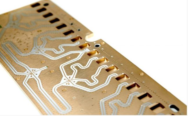
A High Frequency PCB is a specialized printed circuit board designed to operate efficiently at frequencies typically above 500 MHz, often used in RF and microwave applications. As modern electronics continue to push the boundaries of speed and performance, high frequency pcb layout has become critical in ensuring signal integrity, reliability, and overall functionality. Devices in sectors like 5G communication, automotive radar, aerospace, satellite systems, and IoT heavily rely on precise high-speed signal transmission, which demands advanced PCB layout techniques. However, designing for high frequencies introduces significant challenges. Engineers must address issues such as signal loss, electromagnetic interference (EMI), dielectric loss, and controlled impedance. A well-executed high frequency pcb layout not only minimizes these problems but also ensures consistent performance in compact, high-density environments. With the increasing demand for faster and more reliable electronic systems, mastering the principles of high frequency pcb layout is more important than ever.
Understanding High Frequency PCB Layout
To create an effective high frequency pcb layout, it’s essential to first understand what qualifies a circuit as “high frequency” and how signal behavior changes at those frequencies. Generally, high frequency PCBs are defined as those operating above 500 MHz, with some designs reaching into the gigahertz (GHz) range, especially in RF and microwave applications.
Several key electrical parameters must be considered in these designs. The dielectric constant (Dk) of the substrate material affects signal speed and impedance. A stable, low Dk is preferred for consistent performance. Equally important is the dissipation factor (Df), which measures energy loss—lower Df values lead to reduced signal attenuation.
Another critical element in high frequency pcb layout is controlled impedance, which ensures signals travel without distortion. At high frequencies, signal behavior becomes complex—crosstalk, reflections, and electromagnetic radiation can significantly impact performance if not properly managed through thoughtful layout and material selection.
Key Steps in High Frequency PCB Layout Design
Creating a successful high frequency pcb layout requires a systematic design approach that balances electrical performance, manufacturability, and cost. The following key steps form the foundation for reliable high-frequency PCB design:
Pre-layout Planning for High Frequency PCB Layout
Start by defining the critical signal paths and frequency domains. High-speed signals must be clearly identified and routed separately from low-frequency or power circuits. Use functional partitioning to isolate analog, digital, and RF zones, minimizing interference. Professional EDA tools like Altium Designer, Cadence Allegro, and Mentor Graphics offer precise control over trace impedance, layout constraints, and signal integrity simulations—crucial for high-frequency success.
Material Selection for High Frequency PCB Layout: Choosing the Right Material
Standard FR-4 material struggles with high-frequency losses due to its inconsistent dielectric properties. In contrast, materials like Rogers 4350B, Taconic, and Isola offer stable dielectric constants and low dissipation factors, making them ideal for high-frequency designs. Material choice directly impacts signal integrity, insertion loss, and EMI behavior—factors that must be tightly controlled in any high frequency pcb layout.
Layer Stackup Design for High Frequency PCB Layout
A well-structured multi-layer stackup improves EMI shielding and signal integrity. High-speed signals should be routed between closely coupled ground and power planes to provide short, stable return paths. Consistent reference planes reduce noise and enable impedance control across all layers. Pay special attention to return path design, especially when signal layers transition across vias.
High Frequency PCB Layout: Essential Routing Techniques
Keep high-speed traces as short and direct as possible, and maintain length matching for differential pairs. Avoid sharp 90-degree corners—opt for 45-degree bends or curved traces to reduce signal reflection. Use controlled impedance routing (e.g., microstrip for surface layers, stripline for internal layers) and ensure adequate spacing between signal and reference planes to minimize crosstalk.
Power and Ground Management in High Frequency PCB Layout
Use a solid ground plane beneath high-frequency traces to ensure low-impedance return paths. Choose between single-point or multi-point grounding depending on system complexity and frequency. Place decoupling capacitors close to power pins and use multiple values to filter a broad frequency spectrum.
EMI/EMC Control Techniques in High Frequency PCB Layout
To mitigate EMI, apply shielding around sensitive areas and use isolation zones between functional blocks. Maintain continuous ground return paths and avoid stubs or floating planes that can act as antennas. Incorporate filters, termination resistors, and controlled impedance transitions to reduce reflections and emissions.
Advanced Design Considerations in High Frequency PCB Layout
As high-speed systems evolve, advanced techniques and technologies play a critical role in optimizing high frequency pcb layout for compactness, reliability, and signal performance. These methods enable engineers to meet the increasingly demanding requirements of next-generation electronics.
HDI (High Density Interconnect) in High-Frequency PCBs
HDI technology allows for finer trace widths, smaller vias, and denser component placement—ideal for high-frequency applications where board space is limited. In high frequency pcb layout, HDI improves signal routing flexibility while reducing parasitic inductance and capacitance, which are critical at GHz frequencies. It also supports high-layer count designs with better layer transitions and reduced signal degradation.
RF-Specific Layout Considerations
RF circuits require meticulous trace routing and impedance control. Designers must minimize or eliminate stubs, use precise matching networks, and carefully control trace width and spacing. RF traces should be as short as possible and isolated from noisy digital areas. Grounding and shielding are particularly important to prevent coupling and maintain signal purity.
Designing for High-Speed Serial Interfaces
Modern interfaces like USB 3.x, PCIe, and DDR4 operate at several gigabits per second and behave similarly to RF signals. Their traces demand length-matching, tight impedance control, and minimal discontinuities. In high frequency pcb layout, these interfaces must be routed using differential pairs, often requiring tuning stubs, back-drilling, and strict adherence to routing constraints to avoid reflections and timing skew.
Blind/Buried Vias and Laser Drilling
For compact high-frequency boards, blind and buried vias enable interconnects between inner layers without affecting outer layer routing. Laser-drilled microvias reduce via size, lower parasitic inductance, and minimize reflection issues. Their use in high frequency pcb layout supports higher routing density while maintaining signal integrity in miniaturized, high-speed designs.
Common Mistakes to Avoid in High Frequency PCB Layout
Even experienced engineers can encounter pitfalls when working on a high frequency pcb layout, especially as operating frequencies move into the multi-gigahertz range. Avoiding common mistakes is essential for maintaining signal integrity, reducing EMI, and ensuring reliable performance.
Relying on FR-4 at GHz-Level Frequencies
FR-4 is a widely used and cost-effective PCB material, but it suffers from high dielectric loss and inconsistent dielectric constant at higher frequencies. Using it in high frequency pcb layout can result in excessive signal attenuation and phase distortion. For GHz-level designs, advanced materials like Rogers 4350B, Isola, or Taconic should be considered to ensure stable electrical properties.
Over-Widening Traces Without Recalculating Impedance
Widening a trace to reduce resistance may seem like a good idea, but if impedance isn’t recalculated, it can cause mismatches leading to reflections and degraded signal quality. In high-frequency design, controlled impedance must be maintained by balancing trace width, dielectric height, and material Dk values.
Ignoring Return Current Path Integrity
High-frequency signals require well-defined return paths, typically through solid ground planes. If the return path is interrupted—by a split plane, via transition, or poor layout—unwanted noise and radiation may result. Every trace in a high frequency pcb layout should be paired with a continuous return path to minimize EMI and ensure signal integrity.
Misunderstanding Frequency vs Performance Trade-offs
Designers sometimes push for the highest frequency possible without understanding the trade-offs. Higher frequencies increase losses, sensitivity to layout variations, and manufacturing complexity. It’s important to choose a frequency that balances performance, material capability, and design tolerance for optimal results.
Best Practices and Real-World Case Studies in High Frequency PCB Layout
To achieve optimal performance in high frequency pcb layout, it’s crucial to learn from the experience of industry experts and follow field-tested design recommendations. Organizations like NASA and leading manufacturers such as ProtoExpress, PCBWay, and Cirexx have shared valuable insights to help engineers avoid common pitfalls and implement best practices.
Expert Insights and NASA Design Principles
According to NASA’s high-speed PCB design guide, success in high-frequency environments depends on planning for controlled impedance, maintaining solid return paths, and minimizing parasitic effects. The agency emphasizes careful stack-up planning and the use of advanced materials to reduce losses and improve signal integrity in mission-critical systems.
Manufacturer Recommendations: ProtoExpress, PCBWay, Cirexx
-
ProtoExpress recommends using low-Df materials like Rogers 4350B and maintaining tight impedance control throughout all layers.
-
PCBWay highlights the importance of isolating RF zones, using short and direct traces, and avoiding sharp angles in high-speed signal paths.
-
Cirexx suggests leveraging HDI technology, blind/buried vias, and simulation tools to predict signal behavior before fabrication.
These recommendations underscore the importance of a design-first approach in high frequency pcb layout—one that takes materials, stack-up, and routing into account from the outset.
PCBONLINE’s 11 Layout Rules for High Frequency
PCBONLINE outlines 11 critical rules to follow, including:
-
Minimize stubs
-
Ensure consistent impedance
-
Match lengths in differential pairs
-
Place decoupling capacitors as close as possible
-
Avoid right-angle bends
-
Use ground shielding where appropriate
-
Avoid via transitions when possible
-
Route high-speed signals on inner layers (stripline)
-
Use appropriate spacing between traces
-
Plan for clean return current paths
-
Verify with signal integrity simulation tools
Following these principles during the high frequency pcb layout process helps ensure robust performance across a wide range of high-speed applications—from RF modules to 5G infrastructure and beyond.
Helpful Resources & External References for High Frequency PCB Layout
A solid understanding of high frequency pcb layout is best supported by expert-backed references and real-world technical documentation. Below is a curated list of highly recommended resources from authoritative organizations and leading PCB manufacturers, each offering unique insights into high-speed PCB design challenges and solutions.
📘 NASA High-Speed PCB Design Guide (PDF)
This comprehensive guide by NASA outlines critical design principles for high-speed and high-frequency PCBs. It includes guidelines on stack-up planning, controlled impedance routing, and return path management. Ideal for aerospace-grade and mission-critical applications.
📗 Cadence High-Speed PCB Design Guidelines (2024)
Updated for 2024, this guide dives deep into PCB layout strategies, material selection, and simulation tools for achieving optimal performance in GHz-range circuits. A must-read for engineers using Allegro or OrCAD in high frequency pcb layout design.
📘 ProtoExpress HF PCB Knowledgebase
ProtoExpress provides an in-depth knowledgebase covering everything from RF material comparisons to stackup recommendations and real-world design examples. Their resources focus on manufacturability and practical layout techniques.
📗 PCBWay HF PCB Basics
PCBWay offers foundational education on what makes a PCB suitable for high-frequency applications, including how to choose the right materials, deal with EMI, and apply HDI techniques in constrained layouts.
📘 Rogers vs FR-4 Comparison (RushPCB)
This article from RushPCB clearly explains why standard FR-4 often fails in high-frequency designs and how Rogers laminates provide superior performance. A critical read for designers comparing cost vs. performance in high frequency pcb layout projects.
These trusted resources are essential for both novice and experienced designers aiming to build efficient, reliable, and high-performance circuits in today’s frequency-driven electronics world.
FQAs Abut High Frequency PCB Layout
How to design a high frequency PCB?
Designing a high frequency PCB involves several key steps:
-
Material Selection: Use high-performance materials with low dielectric loss (e.g., Rogers, Taconic) for better signal integrity.
-
Controlled Impedance: Ensure precise control of impedance for signal paths, typically 50 ohms for single-ended and 100 ohms for differential pairs.
-
Layer Stackup: Use multi-layer stackups with dedicated ground and power planes to ensure stable return paths and minimize EMI.
-
Trace Routing: Keep traces as short as possible, minimize 90-degree angles, and maintain proper spacing to reduce reflections and crosstalk.
-
Return Path Management: Ensure a continuous, low-impedance return path for high-speed signals to minimize noise and signal degradation.
-
Simulation: Use simulation tools to check signal integrity and power integrity before fabrication.
What is the best PCB material for high frequency?
The best PCB material for high frequency applications includes:
-
Rogers (e.g., Rogers 4350B): Offers a low dielectric constant (Dk) and low dissipation factor (Df), making it ideal for high-frequency and RF circuits.
-
Taconic: Known for low loss and high-frequency stability, it is commonly used in RF and microwave applications.
-
Isola: Provides a range of materials designed for high-speed and high-frequency PCB applications.
-
PTFE (Teflon): Frequently used in aerospace and high-speed communications due to its excellent dielectric properties.
These materials minimize signal loss, maintain consistent impedance, and offer superior performance in high-frequency designs.
What is the highest frequency PCB?
The highest frequency PCB can reach into the GHz (gigahertz) range. While RF PCBs can operate effectively at frequencies up to 40 GHz or more, typical high-frequency PCBs for advanced communication systems like 5G can go up to 100 GHz or higher, depending on the design and material used. The exact limit depends on the materials, stackup, and specific design requirements, but high-frequency PCB designs are generally considered to be above 500 MHz and can go into the tens or hundreds of GHz.
How to design a high-speed PCB?
Designing a high-speed PCB involves:
-
Material Choice: Select materials with low loss and stable impedance characteristics (e.g., FR-4, Rogers, Isola).
-
Layer Stackup: Ensure a proper multi-layer stackup with dedicated power, ground planes, and signal layers.
-
Signal Integrity: Use short, matched traces for differential pairs, and avoid sharp bends or vias that can cause signal reflections.
-
Impedance Control: Maintain controlled impedance for traces, especially for high-speed serial interfaces like PCIe or DDR.
-
Power Distribution: Ensure proper decoupling and minimize power noise through strategic placement of decoupling capacitors.
-
Simulation and Testing: Use simulation tools (e.g., SI and PI analysis) to verify the design for signal integrity and noise issues before manufacturing.
These steps help maintain signal integrity and minimize issues like signal reflection, crosstalk, and EMI in high-speed PCB designs.

