

Key Benefits of Using HDI PCB Board in Modern Electronics
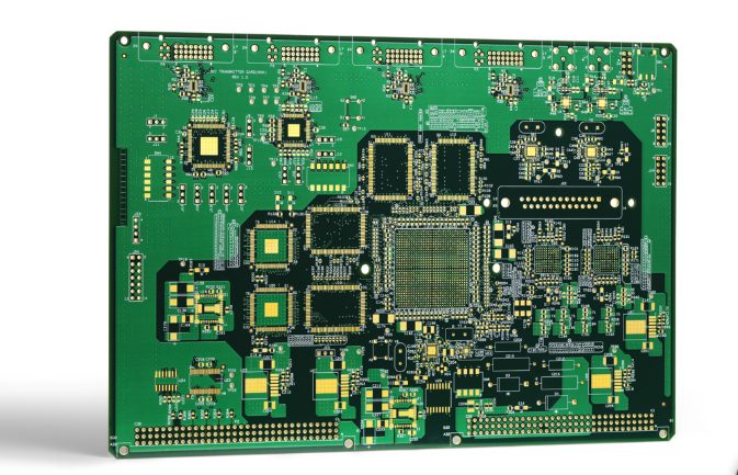
Printed Circuit Board (PCB) technology has evolved significantly over the years, transitioning from basic single-layer boards to complex multi-layer designs capable of supporting high-speed applications. Among these advancements, the HDI PCB board (High-Density Interconnect PCB) has emerged as a critical innovation, enabling the miniaturization of modern electronic devices. An HDI PCB board utilizes microvias, blind vias, and buried vias to achieve higher wiring density and reduce the overall footprint of the PCB. This allows for more compact designs while maintaining superior electrical performance. In today’s advanced electronics, such as smartphones, wearables, and automotive systems, the HDI PCB board plays a vital role by enhancing signal integrity, reducing electromagnetic interference (EMI), and supporting higher-frequency signals. Its ability to increase circuit density and optimize electrical characteristics makes the HDI PCB board indispensable for high-performance, space-constrained applications across various industries.
Understanding HDI PCB Board Technology
The HDI PCB board (High-Density Interconnect PCB) represents an advanced class of printed circuit boards designed to meet the increasing demands of compact, high-performance electronic devices. Characterized by higher wiring densities, smaller vias, and thinner traces, the HDI PCB board allows for the integration of complex circuitry within limited space, making it ideal for modern applications where miniaturization and enhanced electrical performance are essential.
Definition and Characteristics of HDI PCBs
An HDI PCB board uses advanced interconnection technologies to achieve higher circuit density. It incorporates microvias, blind vias, and buried vias to increase the routing space between layers, reducing the need for larger board sizes. The defining characteristics of HDI PCB boards include:
-
Higher Wiring Density: Allows for more components and connections per unit area.
-
Reduced Signal Loss: Improves electrical performance through shorter interconnection paths.
-
Compact Design: Supports miniaturized electronic devices without compromising functionality.
Key Features of HDI PCB Board
Microvias and Blind/Buried Vias
A key feature of the HDI PCB board is its use of microvias, blind vias, and buried vias. Microvias are laser-drilled holes that connect adjacent layers in the PCB, enhancing electrical performance by reducing signal path length. Blind vias connect the outer layer to an inner layer without passing through the entire board, while buried vias connect internal layers, saving space and minimizing crosstalk.
Fine-Line Traces and Spacing
The HDI PCB board leverages fine-line traces and minimal spacing between conductors, which enables higher routing density. Fine-line technology reduces the trace width and spacing to accommodate more interconnections in a smaller area, enhancing signal integrity and minimizing interference. This precision routing capability is essential for high-speed, high-frequency applications.
High Layer Density
Another distinguishing feature of an HDI PCB board is its high layer density, achieved through sequential lamination processes. Multiple signal and power layers can be stacked with minimal spacing, allowing for increased design complexity without compromising performance. This layered structure enhances power distribution and thermal management, ensuring reliability in demanding environments.
Common Applications of HDI PCB Board
The versatility and reliability of HDI PCB boards make them indispensable in various industries, including:
-
Mobile Devices: Smartphones and tablets utilize HDI PCB boards to support high-frequency operations in compact designs.
-
Wearables: Smartwatches, fitness trackers, and other wearable electronics benefit from the miniaturization enabled by HDI PCB boards.
-
Automotive Electronics: Advanced Driver Assistance Systems (ADAS) and infotainment systems rely on HDI PCB boards for seamless performance.
-
Medical Electronics: HDI technology powers miniaturized medical devices such as pacemakers and diagnostic equipment, ensuring precision and reliability.
By leveraging the advanced capabilities of HDI PCB boards, manufacturers can develop more compact, efficient, and high-performance electronic systems tailored for the most demanding applications.
HDI PCB Board Design Guide
Designing an HDI PCB board (High-Density Interconnect PCB) involves a meticulous approach to layer stackup, microvia placement, trace management, and signal integrity to ensure optimal performance in high-speed and high-frequency applications. This section provides a detailed guide on designing an HDI PCB board, covering critical aspects such as layer configurations, microvia strategies, routing techniques, and EMI/EMC management.
Layer Stackup Considerations
The layer stackup is a fundamental element in designing an HDI PCB board as it directly affects signal integrity, thermal management, and overall system performance. Various HDI structures, such as 1+N+1, 2+N+2, and 3+N+3, are used depending on the complexity and performance requirements.
-
1+N+1 Structure:
-
Single microvia layer on both sides of the core layer.
-
Ideal for applications requiring moderate density and signal performance.
-
-
2+N+2 Structure:
-
Two microvia layers per side, providing enhanced routing density.
-
Suitable for high-speed, multi-layer designs where signal integrity is crucial.
-
-
3+N+3 Structure:
-
Three or more microvia layers per side, enabling the highest density of interconnections.
-
Ideal for advanced applications like 5G, IoT, and RF designs where performance is critical.
-
Material Selection:
Selecting suitable materials for an HDI PCB board is essential for maintaining signal integrity and effective thermal management. High-frequency laminates such as FR-4, Rogers, or Isola materials with low dielectric constants (Dk) and low loss tangents (Df) help to minimize signal loss and reduce crosstalk. Additionally, materials with high thermal conductivity ensure reliable heat dissipation, preventing thermal failures in compact, high-density circuits.
Microvia Design and Placement
Microvias play a pivotal role in HDI PCB board design by enabling connections between adjacent layers while minimizing signal path lengths. Proper microvia design and placement are essential for ensuring mechanical and electrical reliability.
-
Aspect Ratio Guidelines:
-
Maintain an aspect ratio (depth-to-diameter) of 1:1 to ensure structural integrity.
-
For microvias, the typical diameter ranges between 75 µm to 150 µm, with a depth not exceeding 100 µm per layer.
-
-
Via-in-Pad Technology:
-
Using via-in-pad technology improves signal performance by reducing parasitic inductance and resistance.
-
Filled and capped vias prevent solder wicking and ensure smooth pad surfaces for component placement.
-
-
Stacked vs. Staggered Microvias:
-
Stacked Microvias: Suitable for high-density designs but require careful control of plating quality to avoid reliability issues.
-
Staggered Microvias: Preferred for higher reliability as they distribute mechanical stress more evenly.
-
Reliability Considerations:
Ensuring robust microvia reliability involves controlling plating quality, minimizing thermal stress, and conducting rigorous thermal cycling tests to prevent via cracking and delamination.
Routing and Trace Management
Routing and trace management are critical in HDI PCB board design to ensure minimal signal degradation and interference. Proper routing techniques contribute to maintaining high-speed performance and preventing signal distortion.
-
High-Speed Signal Routing:
-
Minimize signal path lengths to reduce propagation delay and loss.
-
Route high-frequency signals on inner layers to shield them from external noise.
-
-
Controlled Impedance Design:
-
Implement controlled impedance to maintain signal integrity, especially for differential pairs and high-frequency signals.
-
Use impedance-matched traces to avoid reflections and signal loss.
-
-
Minimizing Crosstalk and Noise:
-
Maintain adequate spacing between adjacent traces to mitigate crosstalk.
-
Implement ground planes between signal layers to reduce noise and improve shielding.
-
Signal Integrity and EMI/EMC Management
Signal integrity and electromagnetic interference (EMI) are critical factors in HDI PCB board design, especially for high-speed applications. Proper design strategies can effectively manage crosstalk, noise, and power distribution to ensure reliable performance.
-
Crosstalk and Noise Mitigation:
-
Use differential pair routing to cancel out noise and improve signal fidelity.
-
Employ shielding techniques, such as ground and power planes, to reduce EMI.
-
-
Power Distribution and Decoupling:
-
Design a well-balanced power distribution network (PDN) to minimize voltage drops.
-
Use decoupling capacitors near critical ICs to filter noise and ensure stable voltage levels.
-
-
Techniques for Signal Distortion Minimization:
-
Maintain consistent impedance across the transmission line.
-
Avoid sharp trace bends and minimize via transitions to reduce signal reflections.
-
By following these guidelines, designers can optimize the performance of an HDI PCB board, ensuring high reliability and superior electrical characteristics for a wide range of advanced applications.
What is the Difference Between HDI PCB Board and Normal PCB?
The HDI PCB board (High-Density Interconnect PCB) is a technological advancement over traditional PCBs, enabling more compact, efficient, and high-performance designs. While normal PCBs follow conventional manufacturing techniques with larger vias and fewer interconnections, the HDI PCB board incorporates advanced microvia technology, fine-line traces, and multiple layers, making it suitable for high-frequency and high-density applications. Understanding the key differences between an HDI PCB board and a normal PCB is essential for selecting the appropriate technology for specific electronic applications.
Density and Miniaturization
One of the primary differences between a HDI PCB board and a normal PCB lies in wiring density and miniaturization.
-
HDI PCB Board:
-
Significantly higher wiring density due to the use of microvias, blind vias, and buried vias.
-
Reduced layer count while maintaining functionality, enabling miniaturization of the overall design.
-
Ideal for compact devices such as smartphones, tablets, and wearables where space is limited.
-
-
Normal PCB:
-
Lower wiring density with larger traces and spacing, resulting in increased board size.
-
Requires more layers to achieve similar functionality, making the design bulkier and less efficient.
-
The compact nature of the HDI PCB board enables more complex and high-speed circuitry in a smaller footprint, improving performance while minimizing the physical size of the device.
Via and Drilling Technology
Another critical distinction between a HDI PCB board and a normal PCB lies in via and drilling technology.
-
HDI PCB Board:
-
Utilizes microvias, blind vias, and buried vias to connect adjacent and internal layers efficiently.
-
Laser drilling is employed to create microvias with diameters as small as 75 µm, allowing for higher routing density.
-
Stacked and staggered microvia structures increase interconnect reliability and reduce signal distortion.
-
-
Normal PCB:
-
Relies primarily on through-hole (PTH) technology, which drills holes through the entire board.
-
Through-hole vias are larger (typically >200 µm in diameter), consuming more space and limiting routing density.
-
Less efficient for high-speed and high-frequency designs due to longer signal paths and higher parasitic inductance.
-
The use of microvias in an HDI PCB board reduces parasitic effects and improves signal performance, making it ideal for high-speed applications.
Performance and Signal Integrity
The HDI PCB board offers superior performance and enhanced signal integrity compared to a normal PCB, making it the preferred choice for advanced applications.
-
HDI PCB Board:
-
Provides excellent signal integrity by reducing signal path lengths and minimizing parasitic capacitance.
-
Superior high-frequency performance with minimal signal distortion, making it suitable for RF, 5G, and IoT applications.
-
Reduces electromagnetic interference (EMI) and crosstalk by implementing controlled impedance and optimized routing techniques.
-
-
Normal PCB:
-
Limited high-frequency performance due to longer signal paths and higher parasitic effects.
-
Increased risk of signal distortion and crosstalk, especially in multi-layer designs with conventional vias.
-
Suitable for low-speed, low-frequency applications where signal integrity is less critical.
-
With its advanced via structures and fine-line routing, the HDI PCB board maintains superior electrical performance and reliability in demanding environments.
Manufacturing Complexity and Cost
Manufacturing complexity and cost are notable differences between a HDI PCB board and a normal PCB.
-
HDI PCB Board:
-
Involves complex processes such as laser drilling, sequential lamination, and copper plating to create microvias and fine-line traces.
-
Requires advanced manufacturing techniques like via-in-pad technology, stacked microvias, and resin-filled vias to ensure reliability and precision.
-
Higher manufacturing cost due to specialized equipment and multiple processing steps.
-
-
Normal PCB:
-
Simpler manufacturing processes using mechanical drilling and through-hole plating for vias.
-
Lower production costs due to conventional fabrication techniques and fewer process steps.
-
Less complexity makes it suitable for lower-density, less demanding applications.
-
Although the cost of producing an HDI PCB board is higher, the benefits in terms of performance, miniaturization, and reliability outweigh the expense for high-end applications.
By leveraging the advanced capabilities of an HDI PCB board, designers can achieve higher performance, reduced form factors, and improved signal integrity, making it the preferred choice for cutting-edge electronic devices.
What is the Difference Between HDI PCB Board and PTH PCB?
The HDI PCB board (High-Density Interconnect PCB) and PTH PCB (Plated Through-Hole PCB) represent two distinct types of printed circuit board technologies used in different applications. While a HDI PCB board focuses on advanced miniaturization and high-frequency performance, a PTH PCB utilizes traditional through-hole technology to establish reliable electrical connections between layers. Understanding the differences between these two technologies is essential for selecting the right PCB type for specific applications.
Definition and Overview of PTH PCB Technology
A PTH PCB (Plated Through-Hole PCB) uses through-hole vias to connect different layers of the board. In this technology, holes are drilled through the entire board, and copper is deposited along the inner walls of the holes to create an electrical connection between layers.
-
Manufacturing Process: Through-hole vias are formed by mechanical drilling, followed by copper plating to establish conductivity.
-
Applications: PTH technology is commonly used in applications where mechanical strength and durability are required, such as industrial controls, power supplies, and automotive systems.
While PTH PCBs provide reliable connections and mechanical stability, they are limited in terms of routing density and miniaturization, making them less suitable for high-speed, compact applications.
Key Differences Between HDI PCB Board and PTH PCB
Manufacturing Process: Laser Microvias vs. Mechanical Drilling
-
HDI PCB Board:
-
Utilizes laser drilling to create microvias with diameters as small as 75 µm.
-
Microvias enable higher wiring density and reduced signal path lengths, ensuring superior electrical performance.
-
Sequential lamination and copper plating processes are employed to form blind and buried vias.
-
-
PTH PCB:
-
Uses mechanical drilling to create larger through-holes that pass through the entire board.
-
The hole diameter typically ranges from 200 µm to 500 µm, limiting the wiring density and increasing the overall board size.
-
Copper is electroplated along the inner walls of the holes to establish electrical continuity.
-
The laser drilling process in an HDI PCB board ensures greater precision and higher via density, allowing for miniaturization and better signal integrity compared to PTH PCBs.
Layer Stackup: HDI with Blind/Buried Vias vs. PTH with Through-Hole Vias
-
HDI PCB Board:
-
Incorporates blind vias (connecting outer layers to inner layers) and buried vias (connecting internal layers without extending to the outer layers), increasing routing efficiency.
-
Multiple microvia layers (e.g., 1+N+1, 2+N+2, 3+N+3) allow for high-density interconnections in a compact form factor.
-
Reduces signal distortion and improves electrical performance due to shorter path lengths and minimized parasitics.
-
-
PTH PCB:
-
Relies exclusively on through-hole vias that extend through the entire PCB, increasing signal path lengths.
-
Layer stackup is typically simpler, with fewer interconnections, leading to lower wiring density.
-
Through-hole vias limit design flexibility and increase the physical size of the board.
-
The advanced stackup of an HDI PCB board allows for high-speed, high-frequency designs while reducing signal loss and electromagnetic interference.
Application Area: HDI for Compact, High-Frequency Circuits vs. PTH for Simpler Designs
-
HDI PCB Board:
-
Ideal for applications requiring miniaturization, high-frequency performance, and high-density routing.
-
Commonly used in smartphones, tablets, wearables, medical devices, and automotive electronics where space and performance are critical.
-
Suitable for RF, 5G, and IoT applications due to its superior signal integrity and compact structure.
-
-
PTH PCB:
-
Used in applications where mechanical durability and reliability are prioritized over miniaturization and high-frequency performance.
-
Commonly applied in power supplies, industrial equipment, and automotive control systems that do not require high wiring density.
-
Suitable for low-frequency, low-complexity designs where space constraints are not a concern.
-
Due to its superior electrical performance and compact design, the HDI PCB board is the preferred choice for high-frequency, high-speed, and space-constrained applications, whereas a PTH PCB is suitable for simpler, lower-density designs.
The primary differences between an HDI PCB board and a PTH PCB lie in their manufacturing processes, layer stackup, and application areas. While the HDI PCB board offers higher wiring density, superior signal integrity, and reduced board size, the PTH PCB provides mechanical stability and reliability for simpler applications. Understanding these differences allows designers to choose the most appropriate technology to meet the specific requirements of their electronic systems.
What is the Difference Between Through-Hole and HDI PCB Board?
The HDI PCB board (High-Density Interconnect PCB) and traditional through-hole PCBs utilize different technologies for interconnections and assembly, leading to distinct advantages in various applications. While through-hole PCBs rely on larger holes and mechanical drilling, the HDI PCB board leverages microvias, blind vias, and buried vias to achieve higher density and superior electrical performance. Understanding these differences helps determine the best choice for specific design requirements.
Structural Differences
The most notable difference between a traditional through-hole PCB and an HDI PCB board lies in the structure and via technology used to establish interconnections between layers.
-
Through-Hole PCB:
-
Utilizes plated through-holes (PTH) that extend through the entire PCB, connecting all layers.
-
Holes are created using mechanical drilling with diameters ranging from 200 µm to 500 µm.
-
Suitable for applications requiring strong mechanical connections, but it limits the routing density and increases board size.
-
-
HDI PCB Board:
-
Incorporates microvias, blind vias, and buried vias to connect layers efficiently without passing through the entire board.
-
Microvias are laser-drilled and have diameters as small as 75 µm, enabling higher routing density.
-
Blind vias connect outer layers to inner layers, while buried vias connect internal layers, improving layer interconnections without increasing board size.
-
Allows for complex multilayer designs (e.g., 1+N+1, 2+N+2, and 3+N+3 structures) that are ideal for compact, high-performance devices.
-
The use of microvias in an HDI PCB board reduces space requirements, allowing for denser circuitry and enhanced electrical performance.
Electrical Performance
The HDI PCB board offers superior electrical performance compared to through-hole PCBs due to reduced parasitic effects and optimized signal paths.
-
Through-Hole PCB:
-
Longer signal paths through through-hole vias result in higher parasitic capacitance and inductance.
-
Increased electromagnetic interference (EMI) and signal distortion, particularly in high-speed circuits.
-
Lower signal integrity due to increased propagation delays and crosstalk between traces.
-
-
HDI PCB Board:
-
Shorter signal paths with microvias reduce parasitic capacitance and inductance, improving signal integrity.
-
Better impedance control and reduced signal loss, making it suitable for high-frequency applications.
-
Supports high-speed signals and minimizes electromagnetic interference (EMI) through optimized layer stackups and advanced routing techniques.
-
The superior electrical characteristics of an HDI PCB board make it the preferred choice for applications requiring high-speed data transmission and low signal distortion.
Assembly and Reliability
Assembly and reliability are also key differentiators between a through-hole PCB and an HDI PCB board, with HDI technology supporting more advanced assembly techniques.
-
Through-Hole PCB:
-
Compatible with Through-Hole Technology (THT), where component leads are inserted through holes and soldered onto the board.
-
Provides strong mechanical connections, making it ideal for applications where durability is a priority.
-
Less suitable for compact designs due to larger component sizes and spacing requirements.
-
-
HDI PCB Board:
-
Supports Surface Mount Technology (SMT), where smaller components are soldered directly onto the surface of the board.
-
Compatible with via-in-pad technology, improving electrical performance by reducing signal path lengths.
-
Higher reliability due to reduced mechanical stress, making it suitable for high-vibration and thermal cycling environments.
-
The use of SMT and via-in-pad technology in an HDI PCB board enhances reliability and performance while enabling miniaturized designs.
Use Cases
The choice between a through-hole PCB and an HDI PCB board depends on the application requirements, with each technology suited to different use cases.
-
Through-Hole PCB:
-
Ideal for power-heavy applications where mechanical strength and durability are critical.
-
Commonly used in industrial equipment, power supplies, and automotive electronics that require strong physical connections.
-
Suitable for low-frequency, low-density circuits where size and performance constraints are less critical.
-
-
HDI PCB Board:
-
Best suited for high-density, high-frequency circuits where miniaturization and performance are essential.
-
Widely used in smartphones, tablets, wearables, medical devices, and automotive ADAS systems where compact designs and reliable electrical performance are required.
-
Preferred for high-speed data transmission and RF applications due to its superior signal integrity and reduced parasitics.
-
By leveraging the advanced capabilities of an HDI PCB board, designers can create compact, high-performance devices that meet the stringent demands of modern electronic applications.
Applications of HDI PCB Board
The HDI PCB board (High-Density Interconnect PCB) is widely used in a variety of industries where miniaturization, high-speed performance, and enhanced reliability are required. Due to its ability to accommodate complex circuitry in a compact form factor while maintaining superior signal integrity, the high-density interconnect PCB plays a crucial role in enabling advanced technologies across consumer electronics, automotive systems, medical devices, and aerospace applications. This section explores the primary applications of this technology in these domains.
Consumer Electronics – Smartphones, Tablets, and Wearables
The HDI PCB board has revolutionized the consumer electronics industry by enabling the development of compact and high-performance devices.
-
Smartphones and Tablets:
-
Modern smartphones and tablets incorporate HDI PCB boards to accommodate high-speed processors, memory chips, and communication modules in a compact space.
-
Microvias, blind vias, and buried vias allow for high-density component placement, enabling enhanced functionality and faster signal transmission.
-
Multiple layer stackups (e.g., 2+N+2 or 3+N+3) provide increased routing efficiency and improved thermal management.
-
-
Wearables and IoT Devices:
-
Smartwatches, fitness trackers, and other wearable devices utilize HDI PCB boards to maintain compact designs without sacrificing performance.
-
High-density routing ensures that sensors, wireless communication modules, and microcontrollers can function efficiently within limited space.
-
HDI technology reduces power consumption, enhancing battery life for wearable devices.
-
By enabling higher functionality in smaller devices, the HDI PCB board plays a pivotal role in the advancement of modern consumer electronics.
Automotive Electronics – Advanced Driver Assistance Systems (ADAS)
The HDI PCB board is essential for modern automotive systems, especially in the implementation of Advanced Driver Assistance Systems (ADAS).
-
ADAS and Autonomous Vehicles:
-
ADAS relies on high-speed processing of sensor data from cameras, LiDAR, radar, and ultrasonic sensors. HDI PCB boards ensure rapid data transmission with minimal latency and interference.
-
Microvia and fine-line routing technologies facilitate the integration of high-frequency signal processing components.
-
Controlled impedance and reduced parasitics contribute to reliable communication between ADAS modules, enhancing safety and performance.
-
-
In-Vehicle Infotainment (IVI) Systems:
-
Modern infotainment systems use HDI PCB boards to manage multiple high-speed data interfaces, ensuring smooth multimedia processing and connectivity.
-
High-density routing and multiple signal layers prevent signal distortion and maintain optimal performance.
-
As automotive systems evolve toward fully autonomous capabilities, the HDI PCB board plays a critical role in ensuring reliable and real-time data processing.
Medical Devices – Miniaturized Devices and Diagnostic Tools
The HDI PCB board is indispensable in the medical industry, where miniaturization and high reliability are essential for diagnostic and therapeutic devices.
-
Implantable and Wearable Medical Devices:
-
Pacemakers, defibrillators, and continuous glucose monitors utilize HDI PCB boards to maintain high functionality in compact designs.
-
High-density routing and microvia technology ensure that critical electronic components are securely integrated while reducing the device footprint.
-
Enhanced signal integrity and low power consumption contribute to the longevity and accuracy of these life-saving devices.
-
-
Diagnostic and Imaging Systems:
-
Advanced diagnostic equipment such as MRI, CT, and ultrasound machines require HDI PCB boards to handle high-frequency signal processing with minimal interference.
-
The ability to reduce signal loss and crosstalk ensures accurate diagnostic results and improved system reliability.
-
With the continued trend toward miniaturization and increased functionality, the HDI PCB board is integral to the advancement of modern medical technologies.
Aerospace and Defense – High-Performance Avionics and Mission-Critical Systems
In the aerospace and defense sectors, the HDI PCB board is used in high-reliability applications that demand superior performance, ruggedness, and signal integrity.
-
Avionics and Communication Systems:
-
Aerospace systems, including avionics control units and communication modules, utilize HDI PCB boards to manage high-frequency signals and ensure reliable data transmission.
-
Multi-layer HDI stackups provide efficient routing and signal isolation, minimizing EMI and ensuring uninterrupted operation.
-
-
Mission-Critical Defense Systems:
-
Radar, missile guidance, and satellite communication systems depend on HDI PCB boards for their ability to handle high-speed data processing with minimal latency.
-
High-temperature tolerance, mechanical durability, and superior electrical performance make HDI PCB boards ideal for mission-critical environments.
-
The use of HDI PCB boards in aerospace and defense applications guarantees consistent performance under extreme conditions, ensuring mission success and operational reliability.
The technology has transformed various industries by enabling miniaturized, high-performance, and reliable electronic systems. Its application in consumer electronics, automotive ADAS, medical devices, and aerospace systems highlights the importance of this innovation in driving progress and enhancing functionality across diverse fields. As electronic devices continue to evolve, the demand for such advanced circuit boards will only grow, shaping the future of cutting-edge technological applications.
Manufacturing Processes for HDI PCB Board
The HDI PCB board (High-Density Interconnect PCB) requires a highly complex and precise manufacturing process to achieve the high wiring density, fine-line traces, and microvia structures necessary for advanced electronic applications. Compared to conventional PCBs, the fabrication of an HDI board involves multiple process steps, including sequential lamination, laser drilling, microvia formation, copper plating, and rigorous quality control. Understanding these processes is essential for ensuring the reliability, durability, and performance of the board in high-frequency and high-speed environments.
Sequential Lamination and Laser Drilling
Sequential lamination and laser drilling are key processes in the fabrication of an HDI PCB board, enabling the creation of complex multilayer structures with high routing density.
-
Sequential Lamination:
-
Sequential lamination is performed to build up the multi-layer stack of an HDI PCB board by laminating multiple core and prepreg layers.
-
After the initial core layer is processed, subsequent layers are sequentially laminated using heat and pressure to bond the dielectric and copper layers.
-
This process is essential for creating high-density interconnections (HDIs) and incorporating blind and buried vias that improve signal routing efficiency.
-
-
Laser Drilling for Microvias:
-
Laser drilling is used to create microvias with diameters as small as 75 µm, connecting adjacent layers with minimal signal loss.
-
Unlike traditional mechanical drilling, laser drilling enables the formation of precise microvias, blind vias, and buried vias with high positional accuracy.
-
Multiple rounds of sequential lamination and laser drilling allow for the creation of stacked and staggered vias, increasing the routing capacity of the HDI PCB board.
-
The combination of sequential lamination and laser drilling ensures the miniaturization of complex circuits while maintaining high electrical performance in an HDI PCB board.
Via Formation and Copper Plating
Via formation and copper plating are critical steps in the HDI PCB board manufacturing process to establish reliable electrical connections between different layers.
-
Microvia Formation and Staggered/Stacked Vias:
-
Microvias are formed using laser drilling technology to create high-density interconnections between adjacent layers.
-
Blind vias connect outer layers to inner layers, while buried vias establish connections between internal layers without extending to the surface.
-
Stacked vias align microvias on multiple layers, enhancing vertical connectivity, while staggered vias provide alternate connection paths for improved signal integrity.
-
-
Copper Plating for Conductive Pathways:
-
After via formation, copper is deposited through an electroless copper plating process to create a conductive layer on the inner walls of the microvias and through-holes.
-
This is followed by electrolytic copper plating, which thickens the copper layer to meet the required thickness for reliable electrical connections.
-
Copper plating ensures uniform conductivity and minimizes resistance, enabling optimal signal transmission in high-speed circuits.
-
The precision of via formation and copper plating processes ensures the structural integrity and electrical reliability of an HDI PCB board, making it ideal for advanced electronic systems.
Inspection and Quality Control Standards
Given the complexity of an HDI PCB board and its critical applications, rigorous inspection and quality control processes are essential to ensure compliance with industry standards and reliability.
-
Automated Optical Inspection (AOI):
-
AOI systems use high-resolution cameras and advanced algorithms to inspect the surface of the HDI PCB board for defects such as misaligned vias, open circuits, and short circuits.
-
AOI helps identify potential issues early in the production process, reducing rework and ensuring high yield rates.
-
-
X-Ray Inspection for Hidden Defects:
-
X-ray inspection is employed to examine the internal layers of the HDI PCB board and detect any defects in microvias, buried vias, or internal traces.
-
This non-destructive method is crucial for verifying the integrity of stacked and staggered vias.
-
-
Electrical Testing and Impedance Control Verification:
-
Electrical testing ensures that all conductive pathways in the HDI PCB board meet design specifications.
-
Impedance control verification is performed to ensure that the high-speed signal paths maintain the desired impedance characteristics, reducing signal distortion and minimizing EMI.
-
-
Thermal and Mechanical Stress Testing:
-
Thermal cycling and mechanical stress tests are conducted to assess the durability and reliability of the HDI PCB board under extreme operating conditions.
-
These tests simulate real-world environments to ensure long-term stability and performance.
-
By adhering to stringent quality control standards, manufacturers ensure that the HDI PCB board meets the highest levels of reliability, performance, and durability required for critical applications.
The manufacturing of an HDI PCB involves a series of highly controlled processes, including sequential lamination, microvia drilling, copper plating, and rigorous quality control. Each step plays a crucial role in ensuring electrical performance, mechanical reliability, and overall quality. As the demand for miniaturized, high-performance devices continues to grow, maintaining precise manufacturing standards becomes even more critical in meeting the evolving needs of advanced electronics.
Advantages and Challenges of HDI PCB Board
The HDI PCB board (High-Density Interconnect PCB) offers numerous advantages that make it the preferred choice for high-performance, miniaturized electronic devices. Its ability to accommodate more components in a smaller footprint while maintaining signal integrity has revolutionized modern electronics. However, despite these benefits, the technology also presents certain challenges, including higher fabrication costs and complex design requirements. This section explores both the advantages and challenges associated with this type of PCB to provide a comprehensive understanding of its role in advanced electronics.
Advantages of HDI PCB Board
Miniaturization and Space-Saving
The HDI PCB board is designed to achieve high-density interconnections, enabling the integration of more functionality within a smaller footprint.
-
Compact Design:
-
By utilizing microvias, blind vias, and buried vias, the HDI PCB board eliminates the need for larger through-holes, freeing up valuable real estate for additional circuitry.
-
Fine-line traces and tighter spacing allow for high component density, reducing the overall size of the board without sacrificing performance.
-
-
Layer Reduction and Cost Efficiency:
-
The ability to achieve high interconnect density means that fewer layers are required to route complex circuits, resulting in a more compact and cost-effective solution.
-
Compared to traditional multilayer PCBs, the HDI PCB board reduces the number of layers required while enhancing functionality.
-
-
Ideal for Portable Devices:
-
The miniaturization capability of the HDI PCB board makes it ideal for applications such as smartphones, tablets, wearables, and IoT devices where space constraints are critical.
-
By leveraging microvia technology and optimized layer stackups, the HDI PCB board significantly reduces the size and weight of electronic devices while enhancing functionality.
Enhanced Electrical Performance and Signal Reliability
The HDI PCB board offers superior electrical performance and improved signal integrity, making it suitable for high-frequency and high-speed applications.
-
Reduced Parasitics:
-
Microvias in an HDI PCB board minimize parasitic capacitance and inductance, improving signal propagation and reducing delays.
-
The shorter signal paths achieved with microvias and fine-line routing reduce signal attenuation and crosstalk.
-
-
Controlled Impedance and Reduced EMI:
-
The precise control of impedance in an HDI PCB board ensures that high-speed signals maintain their integrity, reducing distortion and signal reflection.
-
Advanced routing techniques and optimized layer stackups help mitigate electromagnetic interference (EMI), ensuring clean signal transmission.
-
-
Increased Reliability:
-
The use of via-in-pad technology and staggered/stacked vias in an HDI PCB board enhances the reliability of interconnections, reducing the risk of failure under high mechanical and thermal stress.
-
The superior electrical characteristics of the HDI PCB board make it a preferred choice for applications requiring high-speed data transmission, low signal distortion, and reliable performance.
Challenges of HDI PCB Board
Higher Fabrication Costs
The advanced manufacturing processes and materials required for the HDI PCB board result in higher fabrication costs compared to traditional PCBs.
-
Microvia and Laser Drilling Costs:
-
Microvia formation and laser drilling add complexity and cost to the manufacturing process.
-
Multiple sequential lamination cycles and via stacking contribute to increased production time and expenses.
-
-
Specialized Materials:
-
High-performance dielectric materials with low dielectric constants (Dk) and low loss tangents (Df) are required to ensure signal integrity in high-frequency applications.
-
These specialized materials are more expensive than conventional PCB materials, adding to the overall cost.
-
-
Testing and Quality Control:
-
The stringent inspection and quality control standards applied to an HDI PCB board increase production costs, as advanced testing methods such as X-ray inspection and impedance control verification are required.
-
While the higher costs of HDI PCB board fabrication may be a deterrent for cost-sensitive applications, the benefits it offers often outweigh these additional expenses.
Complex Design and Manufacturing Requirements
Designing and manufacturing an HDI PCB board involves a high level of complexity and requires specialized expertise.
-
Advanced Design Techniques:
-
Designing an HDI PCB board involves precise control of microvia placement, trace routing, and impedance matching to ensure high signal integrity.
-
Signal integrity analysis, crosstalk management, and power distribution network (PDN) optimization are critical in high-frequency HDI designs.
-
-
Sequential Lamination and Via Formation:
-
The sequential lamination process used to build multilayer structures with stacked and staggered vias increases the complexity of fabrication.
-
Microvia stacking and staggered via placement require accurate alignment and drilling precision, adding to manufacturing challenges.
-
-
Thermal Management and Reliability:
-
Proper thermal management techniques must be incorporated to ensure that the HDI PCB board can withstand high-power applications.
-
Ensuring the reliability of stacked microvias and blind/buried vias under mechanical stress and thermal cycling requires rigorous testing and validation.
-
Due to the intricate design and fabrication processes, the HDI PCB board is best suited for applications that demand high performance and reliability, where design complexity is justified by enhanced functionality.
The HDI PCB offers numerous advantages, including miniaturization, space-saving, superior electrical performance, and enhanced signal reliability, making it the ideal choice for high-performance, compact electronic devices. However, these benefits come with challenges, such as higher fabrication costs and complex design requirements, which must be carefully managed to ensure the successful implementation of this technology. As the demand for miniaturized, high-speed electronic systems continues to grow, HDI will play an increasingly critical role in enabling next-generation technologies.
Future Trends and Innovations in HDI PCB Board
As the demand for smaller, faster, and more efficient electronic devices continues to grow, HDI technology is evolving rapidly. New advancements in manufacturing processes, materials, and design techniques are driving the future of HDI development. These innovations are enabling the creation of more compact, high-performance devices across various industries, including wearables, IoT devices, automotive electronics, and medical devices. This section explores the emerging trends and innovations that are shaping the future of HDI technology.
Adoption of mSAP (Modified Semi-Additive Process) for Finer Traces
One of the key advancements in HDI PCB board manufacturing is the adoption of the Modified Semi-Additive Process (mSAP). This process is gaining traction as a way to produce finer traces and achieve even higher circuit densities, which are crucial for modern electronic devices.
-
Finer Line Widths and Greater Density:
-
mSAP allows for the creation of finer line widths, as small as 25 microns, which enables higher density routing. This is especially important in HDI PCB board designs where space is at a premium, and more complex circuitry must fit within a smaller area.
-
By using mSAP, manufacturers can reduce the width of the traces and increase the number of layers without compromising performance, enabling the design of smaller and more powerful devices.
-
-
Improved Precision and Yield:
-
The precision of mSAP ensures that the traces are consistent in size, which improves the overall yield during production.
-
This also reduces the risk of defects that can impact the functionality of the HDI PCB board, such as signal loss or interference.
-
As the mSAP process becomes more widely adopted, it is expected to play a significant role in pushing the limits of HDI PCB board miniaturization and performance, particularly in high-frequency and high-speed applications.
Development of Flex-Rigid HDI PCBs for Wearables and IoT Devices
The growing demand for wearables and IoT devices is driving the development of flex-rigid HDI PCBs, which combine the benefits of flexible and rigid PCB technologies. These advanced HDI PCB board designs offer increased versatility, reliability, and space efficiency for next-generation devices.
-
Flex-Rigid Design for Compactness:
-
Flex-rigid HDI PCB boards enable designers to create devices that are both compact and flexible, allowing for intricate shapes and smaller form factors. This is particularly useful for wearables and IoT devices that require flexibility while maintaining high performance.
-
The ability to fold or bend the PCB in certain areas without sacrificing electrical performance is a game-changer for compact wearable devices like smartwatches, fitness trackers, and medical patches.
-
-
Enhanced Durability for Wearables:
-
In wearables and other mobile devices, the HDI PCB board’s ability to withstand physical stress and flexing is crucial. Flex-rigid HDI PCBs provide the mechanical strength of rigid PCBs with the flexibility of flexible circuits, ensuring reliability and durability.
-
These PCBs are also more resistant to fatigue and wear over time, making them ideal for products that undergo constant movement and flexing.
-
The continued development of flex-rigid HDI PCB board technology is expected to fuel the growth of wearable devices, smart sensors, and IoT devices, offering compact and highly reliable solutions for increasingly complex systems.
Advancements in Materials for Improved Thermal and Electrical Performance
As electronic devices become more powerful, managing heat dissipation and maintaining optimal electrical performance are becoming increasingly important. Innovations in materials for HDI PCB board manufacturing are addressing these challenges and enhancing the performance of high-density interconnect PCBs.
-
Thermal Management Materials:
-
Advanced HDI PCB board materials with improved thermal conductivity are being developed to dissipate heat more efficiently, ensuring that high-performance devices do not overheat.
-
Materials such as ceramic-filled resins, high-Tg epoxy resins, and copper-filled polymers are being integrated into HDI PCB boards to provide better thermal management without compromising the overall size or weight of the device.
-
-
Low-Loss Dielectric Materials for Signal Integrity:
-
To reduce signal loss and maintain signal integrity in high-frequency applications, HDI PCB board manufacturers are using low-loss dielectric materials, which improve electrical performance by minimizing the attenuation of high-speed signals.
-
Materials like PTFE (Polytetrafluoroethylene) and low-Dk (dielectric constant) composites are becoming more common, as they help ensure that high-frequency signals pass through the PCB with minimal degradation.
-
-
High-Performance Copper and Alloy Materials:
-
HDI boards are increasingly being constructed with high-performance copper alloys, which offer better electrical conductivity, reduced resistance, and improved heat dissipation properties.
- These advanced materials contribute to the overall performance of the board, allowing it to handle high-speed, high-frequency signals while maintaining thermal stability.
-
As the demand for high-performance, heat-sensitive devices increases, advancements in materials for HDI PCB boards will continue to play a critical role in improving the overall functionality, reliability, and longevity of next-generation electronic products.
The future of HDI PCB technology is filled with exciting possibilities driven by innovations in manufacturing processes, material science, and design techniques. The adoption of mSAP for finer traces, the development of flex-rigid PCBs for wearables and IoT devices, and advancements in materials for thermal and electrical performance are all contributing to the ongoing evolution of this technology. As these trends continue to unfold, HDI PCBs will remain at the forefront of high-performance electronics, enabling the creation of smaller, faster, and more efficient devices for a wide range of applications.
FQAs Abut HDI PCB Board
What is HDI in PCB?
HDI stands for High-Density Interconnect. It refers to a type of PCB (Printed Circuit Board) design that has a higher wiring density than conventional PCBs. HDI PCBs use advanced techniques like microvias, fine-line traces, and stacked vias to create a compact and efficient layout. These boards are often used in applications where space is limited, such as mobile devices, wearables, and high-performance electronics. HDI PCBs allow for better electrical performance and more components to be packed into a smaller area.
What is the difference between HDI PCB and normal PCB?
The main differences between HDI PCB and a normal PCB are:
-
Density: HDI PCBs offer higher density interconnections, allowing for smaller and more compact designs, while normal PCBs typically have larger traces and fewer components packed into the same area.
-
Via Types: HDI PCBs use microvias, blind vias, and buried vias, which are smaller and more efficient than the traditional through-hole vias used in normal PCBs.
-
Performance: HDI PCBs offer better performance in terms of signal integrity and are ideal for high-speed, high-frequency applications. Normal PCBs may experience more signal loss and interference due to larger vias and traces.
What is the difference between HDI and PTH PCB?
PTH PCB (Plated Through-Hole PCB) and HDI PCB differ mainly in their via technology and manufacturing process:
-
Via Technology: HDI PCBs use microvias, which are much smaller than the traditional through-holes (PTH) found in regular PCBs. Microvias allow for higher routing density and more compact designs. In contrast, PTH PCBs use through-hole vias that are drilled through the entire board, requiring more space.
-
Design Complexity: HDI PCBs support higher density and more complex circuit designs, while PTH PCBs are typically used for simpler designs.
-
Performance: HDI PCBs provide better signal integrity and high-frequency performance compared to PTH PCBs, which may suffer from signal loss and lower reliability in high-speed applications.
What is the difference between through-hole and HDI?
The primary differences between through-hole and HDI (High-Density Interconnect) PCBs are:
-
Via Types: Through-hole PCBs use large vias that are drilled through the entire board, while HDI PCBs use smaller microvias that are typically drilled only partially or just at specific layers. This makes HDI PCBs more compact and efficient.
-
Size and Density: Through-hole PCBs are less dense and require more space for routing compared to HDI PCBs, which allow for higher density interconnections in a smaller footprint.
-
Electrical Performance: HDI PCBs offer superior electrical performance due to their smaller vias and finer traces, leading to reduced signal loss and better signal integrity. Through-hole PCBs are less suitable for high-speed, high-frequency applications.


