

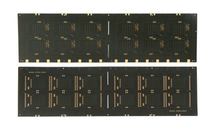
In semiconductor packaging, IC substrates play a crucial role as the interface between the silicon die and the printed circuit board (PCB), ensuring efficient electrical connections, heat dissipation, and mechanical support. As electronic devices become smaller and more complex, the need for high-performance packaging solutions has grown significantly. Among these, Ball Grid Array (BGA) technology has become a dominant choice due to its ability to offer higher pin counts, improved thermal performance, and superior electrical characteristics compared to traditional leaded packages. BGA is widely used in applications ranging from consumer electronics to high-performance computing, where reliability and performance are paramount. To meet the evolving demands of advanced electronics, Custom BGA/IC substrates have emerged as a vital solution. Customization enables manufacturers to optimize substrate designs for specific performance needs, miniaturization challenges, and reliability requirements, ensuring that devices meet the high standards of next-generation applications in AI, IoT, and high-speed computing.
Understanding Custom BGA/IC Substrates vs. Traditional PCBs
Key Differences Between IC Substrates and PCBs
IC substrates and traditional printed circuit boards (PCBs) may seem similar, but they serve different functions in electronic packaging. PCBs are designed for general electronic circuit connections, providing mechanical support and electrical pathways for various components. In contrast, IC substrates act as an intermediary between the silicon die and the PCB, ensuring enhanced electrical performance, miniaturization, and reliability. Custom BGA/IC substrates are specifically engineered to meet the demands of high-density and high-speed applications, offering superior interconnect technology compared to standard PCBs.
Materials and Structure Comparison
Traditional PCBs typically use fiberglass-reinforced epoxy laminates (such as FR4), while IC substrates employ high-performance materials like Ajinomoto build-up film (ABF) or BT (Bismaleimide-Triazine) resin. These advanced materials allow Custom BGA/IC substrates to achieve finer line spacing, higher wiring density, and better electrical insulation. Additionally, IC substrates often incorporate multi-layer designs with microvias, laser-drilled vias, and embedded passive components, which are less common in standard PCB structures.
Application Areas and Performance Differences
PCBs are commonly used in low-to-medium complexity devices, including consumer electronics, automotive systems, and industrial equipment. In contrast, Custom BGA/IC substrates are essential for high-performance computing, AI accelerators, 5G communications, and compact wearable devices. Their ability to support high-frequency signals, efficient heat dissipation, and miniaturized form factors makes them indispensable in advanced semiconductor packaging.
What is IC Package Substrate in Custom BGA/IC Substrates?
Definition and Function in Semiconductor Packaging
IC package substrates are a crucial component in semiconductor packaging, serving as the bridge between the silicon die and the printed circuit board (PCB). These substrates provide electrical connections, mechanical support, and thermal management, ensuring optimal performance and reliability of integrated circuits. Unlike traditional PCBs, IC substrates feature high-density interconnects (HDI) and advanced material compositions to support the increasing complexity of modern semiconductor devices. In Custom BGA/IC substrates, these advanced packaging solutions are tailored to meet specific design requirements, enhancing signal integrity, reducing power loss, and improving overall efficiency.
Different Types of IC Package Substrates
There are several types of IC package substrates, each designed for specific applications:
- FC-BGA (Flip-Chip Ball Grid Array): Used in high-performance computing and AI processors, offering improved thermal and electrical performance.
- CSP (Chip Scale Package): A compact solution for mobile and wearable devices, enabling miniaturization while maintaining functionality.
- SiP (System-in-Package): Integrates multiple chips into a single package for applications like 5G, IoT, and advanced computing.
- Wire Bond Substrates: Common in cost-sensitive applications, connecting the chip to the substrate via thin bonding wires.
Advantages of Using High-Density Interconnect (HDI) Substrates
HDI substrates are essential for Custom BGA/IC substrates, as they allow for finer line widths, smaller via sizes, and higher wiring density. These features enable:
- Better electrical performance: Reduced signal loss and lower electromagnetic interference (EMI).
- Miniaturization: Compact designs for high-performance computing, mobile devices, and medical applications.
- Enhanced thermal management: Improved heat dissipation, critical for power-intensive semiconductor applications.
By leveraging Custom BGA/IC substrates with HDI technology, manufacturers can achieve superior performance, increased reliability, and optimized packaging solutions for next-generation electronics.
Ball Grid Array (BGA) and Its Variants in Custom BGA/IC Substrates
Explanation of BGA Technology and Its Benefits
Ball Grid Array (BGA) is a widely used semiconductor packaging technology that offers superior electrical performance, higher component density, and improved thermal dissipation compared to traditional leaded packages. In a BGA package, solder balls are arranged in a grid pattern beneath the chip, allowing for a greater number of electrical connections within a compact footprint. This design minimizes signal interference and enhances mechanical stability, making it ideal for applications in high-performance computing, networking, and consumer electronics.
In Custom BGA/IC substrates, BGA technology is tailored to specific design requirements, optimizing signal integrity, power efficiency, and thermal management. Customization enables fine-tuning of solder ball pitch, substrate material selection, and layer design to enhance the performance and reliability of advanced semiconductor devices.
Differences Between Standard BGA and Micro BGA (μBGA)
Standard BGA packages are designed for applications requiring high pin counts and robust mechanical strength, commonly used in processors, memory modules, and graphic chips. However, as electronic devices continue to shrink, the need for more compact packaging solutions has led to the development of Micro BGA (μBGA).
μBGA differs from standard BGA in the following ways:
- Size: μBGA packages are significantly smaller, making them suitable for mobile and wearable devices.
- Ball Pitch: μBGA has a finer pitch between solder balls, allowing for greater miniaturization.
- Manufacturing Process: μBGA often utilizes advanced substrate materials and redistribution layers (RDL) to accommodate higher interconnect density.
In Custom BGA/IC substrates, manufacturers can modify BGA and μBGA designs to meet specific application needs, ensuring optimal performance in compact electronic devices.
How FC-BGA (Flip-Chip BGA) Improves Electrical and Thermal Performance
Flip-Chip BGA (FC-BGA) is an advanced BGA variant that further enhances electrical and thermal performance by directly mounting the semiconductor die onto the substrate with conductive bumps instead of wire bonding. This direct connection reduces resistance and inductance, resulting in:
- Higher Signal Speeds: FC-BGA minimizes parasitic capacitance and inductance, improving signal integrity for high-frequency applications.
- Better Thermal Dissipation: Heat is efficiently transferred through the substrate, preventing thermal buildup in high-power components.
- Compact Design: Eliminates the need for long bond wires, reducing overall package height and enabling thinner devices.
In Custom BGA/IC substrates, FC-BGA technology is particularly beneficial for high-performance computing, AI accelerators, and advanced telecommunications equipment, where efficient heat dissipation and high-speed signal transmission are crucial.
Customization of BGA/IC Substrates in Custom BGA/IC Substrates
Key Design Considerations
Customizing BGA/IC substrates involves multiple design factors that directly impact performance, durability, and integration capabilities. In Custom BGA/IC substrates, the following key aspects must be considered:
- Layer Count: Depending on the complexity of the IC package, substrates may have multiple layers to support high-density routing and power distribution. High-performance applications, such as AI accelerators and data center processors, often require substrates with 8–20 layers.
- Material Selection: The choice of materials, such as BT (Bismaleimide-Triazine) resin or Ajinomoto Build-up Film (ABF), is critical for electrical insulation, heat dissipation, and mechanical strength.
- Via Technology: Different via structures, including through-hole vias (THV), microvias, and buried vias, enable efficient routing in multilayer substrates. Microvias are especially important in HDI (High-Density Interconnect) substrates for finer circuit integration.
- Pitch Size: The solder ball pitch in BGA packages determines interconnect density. Advanced Custom BGA/IC substrates may have pitches as small as 0.3 mm to accommodate ultra-miniaturized devices.
Advanced Manufacturing Techniques
To achieve high performance and reliability, Custom BGA/IC substrates require advanced fabrication processes, including:
- Substrate Etching: This process defines fine circuit patterns on the substrate to enable high-density wiring while ensuring minimal signal loss.
- Laser Drilling: Used to create precise microvias, laser drilling enhances electrical connectivity and supports HDI structures.
- Electroplating: Electrochemical deposition of copper ensures strong interconnects and improves conductivity for high-frequency signals. This step is crucial in reducing resistance and enhancing signal integrity in high-speed computing and RF applications.
Performance Optimization for Specific Applications
Different industries demand specific performance optimizations in Custom BGA/IC substrates:
- High-Speed Computing: AI processors and data center chips require substrates with low signal loss, high power efficiency, and superior thermal dissipation.
- AI Chips: Advanced packaging solutions integrate high-bandwidth memory (HBM) and multiple chiplets to maximize AI processing capabilities.
- RF Applications: Wireless communication devices, including 5G infrastructure, need substrates with excellent high-frequency performance, low dielectric loss, and minimal crosstalk.
By leveraging advanced customization techniques, Custom BGA/IC substrates provide tailored solutions that enhance device performance, reduce power consumption, and enable next-generation semiconductor applications.
Applications of Custom BGA/IC Substrates
Consumer Electronics: Custom BGA/IC Substrates in Smartphones, Laptops, and Gaming Consoles
Consumer electronics demand compact, high-performance, and power-efficient semiconductor solutions. Custom BGA/IC substrates enable advanced packaging for processors, memory chips, and graphics units in devices such as smartphones, laptops, and gaming consoles. In these applications, miniaturization and high-speed data processing are critical. BGA substrates provide excellent electrical connections, efficient heat dissipation, and reduced signal interference, ensuring smooth performance in high-resolution displays, AI-driven features, and fast-charging systems.
Automotive and Industrial Applications of Custom BGA/IC Substrates
Modern automotive systems rely on complex electronic components, including advanced driver-assistance systems (ADAS), infotainment systems, and electric vehicle (EV) power management. Custom BGA/IC substrates play a crucial role in improving the reliability and durability of automotive chips, which must operate under extreme temperatures and harsh conditions. In industrial automation, these substrates support high-speed processing units in robotics, machine learning applications, and real-time monitoring systems, enhancing precision and efficiency in manufacturing.
Medical Devices and Wearables: The Role of Custom BGA/IC Substrates
Medical electronics and wearable devices require compact, lightweight, and highly reliable semiconductor solutions. Custom BGA/IC substrates are essential for miniaturized chip designs in hearing aids, pacemakers, blood pressure monitors, and wearable health trackers. These substrates ensure stable signal transmission, low power consumption, and resistance to environmental factors such as moisture and temperature fluctuations, making them ideal for long-term and continuous use in medical applications.
High-Performance Computing and AI-Driven Devices: Custom BGA/IC Substrates in Advanced Technology
High-performance computing (HPC) and artificial intelligence (AI) applications require advanced semiconductor packaging solutions to handle massive data processing tasks with minimal latency. Custom BGA/IC substrates support high-density interconnects, low-power operation, and superior thermal management for data center processors, AI accelerators, and graphics processing units (GPUs). By optimizing signal integrity and reducing electromagnetic interference (EMI), these substrates enable faster computation speeds and improved efficiency for AI-driven applications in cloud computing, big data analytics, and deep learning.
With their versatility and adaptability, Custom BGA/IC substrates are revolutionizing various industries, ensuring the next generation of electronics meets the growing demands for performance, efficiency, and reliability.
Challenges in Manufacturing and Solutions for Custom BGA/IC Substrates
Miniaturization and Fine-Pitch Challenges
As semiconductor devices continue to shrink, Custom BGA/IC substrates must accommodate increasingly fine-pitch interconnects and high-density wiring. The challenge lies in maintaining manufacturing precision while ensuring electrical reliability. Traditional PCB fabrication methods struggle with ultra-fine traces and microvia structures, leading to potential signal loss or defects.
Solution:
- Adoption of high-density interconnect (HDI) technology with laser-drilled microvias, enabling tighter spacing and improved routing density.
- Use of advanced photolithography techniques to create finer circuit patterns without compromising electrical performance.
- Implementation of automated optical inspection (AOI) and X-ray inspection to detect defects in micro-scale structures.
Thermal Management and Heat Dissipation Solutions
With the increasing power demands of AI chips, high-performance computing (HPC), and 5G processors, Custom BGA/IC substrates must efficiently dissipate heat to prevent performance degradation and failure. Poor thermal management can lead to chip overheating, reduced lifespan, and potential system instability.
Solution:
- Integration of thermal vias and metal heat spreaders to enhance heat dissipation.
- Use of high thermal conductivity substrate materials, such as copper-clad laminates or embedded heat sinks.
- Adoption of flip-chip BGA (FC-BGA) technology, which reduces thermal resistance by directly connecting the chip to the substrate.
Signal Integrity and Power Integrity Considerations
High-speed computing, RF applications, and AI accelerators require Custom BGA/IC substrates that ensure stable signal transmission and power delivery. Electromagnetic interference (EMI), crosstalk, and voltage fluctuations can lead to performance bottlenecks and data errors.
Solution:
- Use of low-dielectric loss materials such as Ajinomoto Build-up Film (ABF) to maintain signal integrity at high frequencies.
- Embedded decoupling capacitors and optimized power distribution networks (PDNs) to reduce power fluctuations.
- Ground plane and shielding techniques to minimize electromagnetic interference and crosstalk.
Reliability Testing and Quality Control
Ensuring long-term reliability is a critical challenge in manufacturing Custom BGA/IC substrates, especially for applications in automotive, aerospace, and medical devices where failure is not an option. Factors such as solder joint fatigue, material delamination, and environmental stress can impact durability.
Solution:
- Comprehensive reliability testing, including thermal cycling, humidity resistance, and mechanical stress testing.
- X-ray inspection and scanning acoustic microscopy (SAM) to detect hidden defects in multi-layer substrates.
- Stringent quality control standards, such as IPC Class 3 and automotive-grade AEC-Q100 certification, to ensure consistency and durability.
By addressing these challenges with advanced manufacturing techniques and rigorous quality control, Custom BGA/IC substrates continue to evolve, meeting the demands of next-generation electronics with improved performance, reliability, and efficiency.
Leading Companies and Innovations in Custom BGA/IC Substrates
Overview of Key Manufacturers
The demand for Custom BGA/IC substrates has led to the emergence of several key players specializing in advanced packaging solutions. Leading manufacturers include:
- Kyocera – A pioneer in high-performance ceramic and organic IC substrates, Kyocera focuses on FC-BGA and other high-density interconnect (HDI) solutions to enhance semiconductor performance.
- Toppan – A leader in FC-BGA and CSP (Chip Scale Package) substrates, Toppan integrates advanced materials and fine-line technology to enable miniaturization and improved thermal management.
- iPCB – Specializing in customized IC substrates, iPCB offers a broad range of solutions, including HDI substrates and high-frequency RF substrates for 5G and AI applications.
- Shinko Electric Industries – A supplier of innovative semiconductor packaging solutions, including advanced FC-BGA and SiP (System in Package) substrates for high-performance computing.
- Unimicron and Ibiden – These companies focus on ultra-thin, high-layer count substrates for AI chips, high-speed networking, and automotive applications.
Emerging Trends in IC Substrate Technology
With the continuous advancement of semiconductor packaging, Custom BGA/IC substrates are evolving to meet the needs of next-generation applications. Some key trends include:
- High-Density Build-Up (HDBU) Substrates – Enabling extremely fine-pitch interconnects for AI processors, data center chips, and mobile SoCs.
- Embedded Active and Passive Components – Reducing footprint and improving performance by integrating capacitors, resistors, and other components directly into the substrate.
- Heterogeneous Integration and Chiplets – The shift from monolithic chip design to multi-chip packaging requires advanced substrate technology to facilitate efficient inter-chip communication.
- 5G and mmWave Optimization – Specialized Custom BGA/IC substrates are being developed with low-loss dielectric materials to support high-frequency RF applications.
Future Developments in Organic and Inorganic Substrates
The future of Custom BGA/IC substrates lies in the continued refinement of both organic and inorganic materials:
- Organic Substrates: Innovations in Ajinomoto Build-up Film (ABF) and other polymer-based materials are enabling thinner, lighter, and higher-performance substrates for consumer electronics and AI-driven applications.
- Inorganic Substrates: Advanced ceramic and silicon-based substrates are gaining traction for extreme environments, such as automotive, aerospace, and quantum computing, due to their superior thermal and electrical properties.
- Hybrid Approaches: The combination of organic and inorganic materials in a single Custom BGA/IC substrate could unlock new possibilities for ultra-high-speed and high-power applications, balancing cost, performance, and reliability.
As manufacturers continue to push the boundaries of Custom BGA/IC substrates, these innovations will shape the future of semiconductor packaging, enabling faster, more efficient, and more compact electronic devices.
Choosing the Right Custom BGA/IC Substrate Partner
Factors to Consider When Selecting a Supplier
Selecting the right manufacturing partner for Custom BGA/IC substrates is critical to ensuring product reliability, performance, and scalability. Companies must evaluate suppliers based on several key factors:
- Manufacturing Capabilities – Assessing whether the supplier can produce fine-pitch substrates, high-density interconnects (HDI), and multi-layer substrates is essential for advanced applications.
- Material Expertise – Different applications require specific materials, such as Ajinomoto Build-up Film (ABF) for high-speed computing or ceramic-based substrates for automotive and aerospace use.
- Customization Flexibility – A reliable partner should offer tailored solutions, including specific layer counts, via structures, and substrate thicknesses, to meet the unique needs of AI chips, RF devices, and data center processors.
- Production Scalability – The supplier should be able to handle both prototyping and mass production while maintaining consistent quality and performance.
- R&D and Innovation – Working with a manufacturer that invests in next-generation packaging technologies ensures long-term competitiveness in the rapidly evolving semiconductor industry.
Cost vs. Performance Trade-offs
While cost is a crucial consideration, prioritizing price over performance can lead to long-term reliability issues. Companies sourcing Custom BGA/IC substrates must balance:
- Material Costs vs. Electrical Performance – Higher-grade materials improve signal integrity and thermal management but come at a premium. Cost-sensitive applications may require alternative laminates or copper-clad solutions.
- Manufacturing Complexity vs. Yield Rates – Advanced features such as microvias, embedded components, and ultra-fine line widths can improve performance but may reduce yield rates, increasing production costs.
- Standardization vs. Customization – While off-the-shelf BGA substrates may be more affordable, custom solutions offer optimized power delivery, heat dissipation, and form factor compatibility for specialized applications.
Quality Certifications and Industry Standards
A trustworthy Custom BGA/IC substrates supplier should comply with stringent industry certifications and quality control measures to guarantee product durability and reliability:
- ISO 9001 & ISO 14001 – Ensuring standardized quality management and environmental responsibility in manufacturing processes.
- IATF 16949 – A critical certification for automotive-grade substrates, ensuring adherence to high-reliability standards.
- IPC-6012/6016 Standards – Defining the quality and performance requirements for rigid and high-density interconnect (HDI) substrates.
- AEC-Q100 & MIL-PRF Standards – Essential for automotive, aerospace, and defense applications where extreme conditions require robust and highly durable substrates.
- RoHS & REACH Compliance – Ensuring environmentally friendly production with restrictions on hazardous substances.
By carefully selecting a Custom BGA/IC substrates manufacturing partner based on these criteria, companies can optimize cost, quality, and performance while ensuring long-term reliability in high-performance semiconductor applications.
FQAs Abut Custom BGA/IC substrates
What is the difference between IC substrate and PCB?
- An IC substrate is a specialized type of substrate used to support integrated circuits (ICs), providing electrical connections between the IC and external components while managing heat dissipation and ensuring signal integrity. It typically has more layers, smaller pitches, and specific material properties suited for high-performance semiconductors.
- A PCB (Printed Circuit Board), on the other hand, is a broader term for a flat board that holds electronic components and connects them using conductive pathways. While a PCB can be used to support ICs, it is generally less specialized than an IC substrate and may not have the necessary properties for high-density interconnections or fine-pitch components.
Is a BGA an IC?
A BGA (Ball Grid Array) is not an IC itself but a type of packaging used for ICs. It refers to a specific arrangement of solder balls on the underside of an integrated circuit package, used to connect the IC to the PCB. BGAs are widely used for packaging ICs due to their ability to offer high-density interconnects and better thermal management.
What is IC package substrate?
An IC package substrate is the material on which an integrated circuit (IC) is mounted and connected. It provides the electrical interconnection between the IC and the PCB, as well as thermal and mechanical support. It is typically made from high-performance materials like epoxy resin, ceramic, or laminate, and it plays a critical role in ensuring the IC’s reliability and functionality in a circuit.
What is the difference between BGA and micro BGA?
The main difference between a BGA (Ball Grid Array) and a micro BGA (μBGA) lies in the size of the solder ball pitch. A standard BGA typically has a pitch of 1.0 mm or larger, while a micro BGA has a smaller pitch, usually around 0.8 mm or smaller. The reduced pitch in micro BGA allows for higher density interconnects and is commonly used in smaller, more compact devices where space is at a premium, such as in mobile phones or wearable electronics.