Custom QFN/QFP Lead Frame

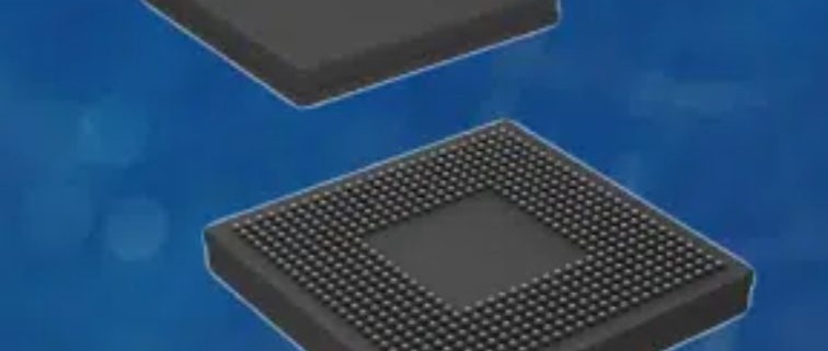
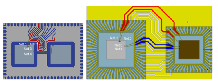
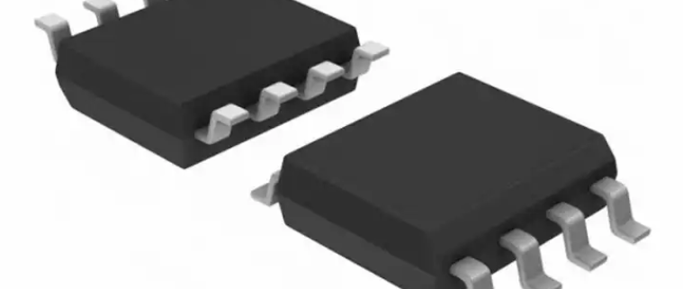
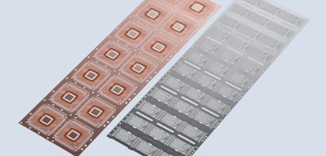
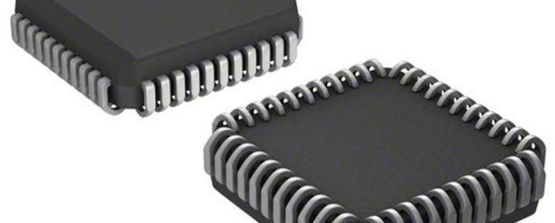
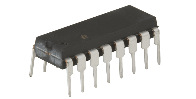
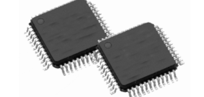
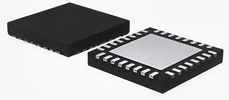
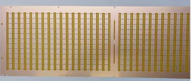
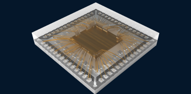
Lead frames are essential components in semiconductor packaging, providing both mechanical support and electrical connections between the silicon chip and the external circuit board. As electronics evolve towards smaller, more powerful devices, the need for advanced lead frame solutions has grown. Custom QFN/QFP Lead Frame designs play a crucial role in this, offering optimized thermal performance, electrical conductivity, and design flexibility. QFN (Quad Flat No-Lead) lead frames are ideal for applications requiring enhanced heat dissipation and reduced signal interference, while QFP (Quad Flat Package) lead frames provide secure soldered connections with extended leads for reliable assembly. The ability to customize these lead frames allows manufacturers to meet specific application needs, improving device performance and longevity. As semiconductor packaging technology advances, custom lead frame solutions will continue to be vital for developing next-generation electronic products. 阅读更多

Custom FCBGA Package Substrate Service

FCBGA (Flip-Chip Ball Grid Array) is an advanced semiconductor packaging technology where the chip is flipped upside down and soldered directly onto a substrate with an array of solder balls, allowing for efficient electrical connections and superior thermal management. This packaging technology plays a vital role in modern electronics by enabling high-density interconnections, smaller form factors, and improved performance. FCBGA is essential in industries such as telecommunications, automotive, and consumer electronics, where there is a constant demand for faster, more reliable, and power-efficient devices. With these requirements in mind, Custom FCBGA Package Substrate Service has become crucial in tailoring substrates to meet specific performance, size, and thermal needs, supporting a broad range of applications. 阅读更多

Multi-Chip Leadframe

Semiconductor packaging is essential for protecting and interconnecting devices, ensuring reliability and performance. As electronic systems grow more complex, multi-chip packaging has become a key solution, integrating multiple chips into a single package to reduce footprint, enhance electrical performance, and improve thermal management. Among various approaches, leadframe-based designs offer a cost-effective and efficient alternative to substrate-based solutions. The leadframe provides mechanical support and electrical connections while facilitating signal transmission and heat dissipation. This makes it particularly valuable in high-performance and miniaturized electronics. One advanced packaging method leveraging these benefits is Multi-Chip Leadframe, which simplifies manufacturing while maintaining high functionality. As demand for compact, high-performance semiconductor solutions continues to rise, this technology remains a crucial driver of innovation in the industry. 阅读更多

Small Outline Integrated Circuit (SOIC)

The Small Outline Integrated Circuit (SOIC) is a widely used surface-mount IC package that offers reduced size, improved thermal performance, and enhanced electrical characteristics compared to traditional through-hole components. Its compact and standardized form factor makes it ideal for both consumer and industrial electronics. In modern electronics, the SOIC plays a crucial role in miniaturization, enabling the design of smaller, lightweight devices. Its compatibility with automated soldering processes ensures cost-effectiveness and reliability in high-volume production. Extensively used in PCB design, the SOIC is found in applications like microcontrollers, memory chips, and analog circuits, particularly in automotive electronics, communication systems, and medical devices, where space-saving and high-performance integration are essential.

阅读更多

TSOP/LOC Lead Frame

Semiconductor packaging plays a crucial role in the electronics industry, ensuring the protection, connectivity, and thermal management of integrated circuits (ICs). Among various packaging technologies, TSOP/LOC Lead Frame is widely used due to its reliability and cost-effectiveness.

A lead frame is a metal structure that provides mechanical support and electrical connections for semiconductor chips. It acts as a bridge between the silicon die and the external circuitry, facilitating efficient signal transmission and heat dissipation. This specific type of lead frame is used in Thin Small Outline Package (TSOP) and Lead-On-Chip (LOC) packaging, both essential for high-density, low-profile semiconductor devices.

TSOP is a compact and thin package commonly used for memory devices like NAND and NOR Flash, while LOC technology enhances performance by placing leads directly on the chip surface. Together, TSOP/LOC Lead Frame solutions offer excellent electrical performance and space efficiency, making them a preferred choice in modern semiconductor applications.

阅读更多

Plastic Leaded Chip Carrier (PLCC) Lead Frame

Plastic Leaded Chip Carrier (PLCC) Lead Frame is a semiconductor packaging technology designed for efficient, reliable IC connections. This surface-mount package features J-leads, offering mechanical support and electrical connectivity in a compact form. PLCC is significant in electronics as it allows for high-density PCB designs and can be used with surface-mount technology (SMT) or in sockets for easy replacement. Its versatility makes it ideal for applications like microcontrollers, memory chips, and logic devices, requiring durability, reusability, and high thermal performance. The purpose of this article is to provide a detailed exploration of PLCC, discussing its structure, manufacturing process, advantages, and key applications in the modern electronics industry.
阅读更多

Plastic Dual In-line Package(PDIP) Lead Frame

The Plastic Dual In-line Package(PDIP) Lead Frame is a widely used electronic packaging solution, known for its versatility and cost-effectiveness. PDIP features two parallel rows of pins, allowing for easy insertion into printed circuit boards (PCBs), making it ideal for through-hole mounting and manual soldering. Its importance in the electronics industry lies in its reliability, durability, and ability to house various types of integrated circuits, such as microcontrollers and operational amplifiers. This article aims to provide a comprehensive analysis of the Plastic Dual In-line Package(PDIP) Lead Frame, exploring its structure, manufacturing process, and role in enhancing the performance of PDIP packages, offering insights into its continued use in consumer electronics, industrial control systems, and more.

阅读更多

Thin Quad Flat Pack Lead Frame

IC packaging is the process of enclosing semiconductor chips in a protective case to ensure electrical connections and mechanical stability. It plays a crucial role in determining the performance, reliability, and integration of integrated circuits (ICs) in electronic devices. One widely used packaging type is the Thin Quad Flat Pack Lead Frame (TQFP), a surface-mount technology that features a square-shaped package with leads extending from all four sides.

This packaging design is specifically created to accommodate high-pin-count ICs while maintaining a thin profile, making it ideal for compact electronic devices. Its lightweight structure, excellent heat dissipation, and ease of PCB assembly contribute to its popularity. The semiconductor industry favors this packaging due to its cost-effectiveness, space efficiency, and reliable electrical performance, making it a preferred choice for consumer electronics, automotive systems, industrial controls, and telecommunications applications.

阅读更多

Quad Flat Non-Lead Frame

In semiconductor packaging, the Quad Flat Non-Lead Frame (QFN) has become a widely used solution for modern electronics. Semiconductor packaging plays a crucial role in protecting integrated circuits (ICs), ensuring electrical connections, and enabling efficient heat dissipation. Traditional leaded packages, such as Dual In-Line Packages (DIP) and Quad Flat Packages (QFP), have been widely used, but as electronic devices become more compact and power-efficient, new packaging technologies are required.

The package is particularly important in today’s electronics due to its small form factor, excellent thermal performance, and low electrical resistance. Compared to leaded packages, it offers significant advantages, including reduced parasitic inductance, enhanced heat dissipation through an exposed die pad, and cost-effective manufacturing. These benefits make it a preferred choice for high-performance applications, including consumer electronics, automotive systems, and industrial devices. As technology advances, this packaging type will continue to play a vital role in semiconductor packaging.

阅读更多

AU/Silver QFN/QFP Lead Frame

QFN (Quad Flat No-Lead) and QFP (Quad Flat Package) are two popular surface-mount IC packaging types, each offering distinct advantages. QFP features extended leads on all four sides for easy inspection and soldering, while QFN is a leadless package known for its superior thermal and electrical performance due to direct pad connections to the PCB. In semiconductor packaging, the lead frame plays a crucial role by providing electrical connections and structural support, ensuring efficient signal transmission, heat dissipation, and mechanical stability. Among the various materials used, AU/Silver QFN/QFP Lead Frame is highly preferred due to its excellent electrical conductivity, thermal properties, and resistance to oxidation. Gold (AU) enhances durability and reliability, while silver (Ag) offers a cost-effective solution with strong conductivity, making AU/Silver QFN/QFP Lead Frame the ideal choice for high-performance applications in consumer electronics, automotive, and industrial sectors.

阅读更多