
TSOP/LOC Lead Frame and Its Role in Semiconductor Packaging
Semiconductor packaging plays a crucial role in the electronics industry, ensuring the protection, connectivity, and thermal management of integrated circuits (ICs). Among various packaging technologies, TSOP/LOC Lead Frame is widely used due to its reliability and cost-effectiveness.
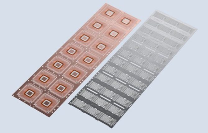
A lead frame is a metal structure that provides mechanical support and electrical connections for semiconductor chips. It acts as a bridge between the silicon die and the external circuitry, facilitating efficient signal transmission and heat dissipation. This specific type of lead frame is used in Thin Small Outline Package (TSOP) and Lead-On-Chip (LOC) packaging, both essential for high-density, low-profile semiconductor devices.
TSOP is a compact and thin package commonly used for memory devices like NAND and NOR Flash, while LOC technology enhances performance by placing leads directly on the chip surface. Together, TSOP/LOC Lead Frame solutions offer excellent electrical performance and space efficiency, making them a preferred choice in modern semiconductor applications.
Basics of TSOP/LOC Lead Frame
Overview of TSOP
TSOP (Thin Small Outline Package) is a widely used semiconductor packaging type designed for high-density memory chips such as DRAM and Flash memory. Due to the increasing demand for compact and high-performance electronic devices, TSOP has become a preferred choice in applications requiring space efficiency and reliable electrical performance.
One of the key features of TSOP is its thin profile, which allows for a significant reduction in package height compared to traditional packaging solutions. Additionally, TSOP packages utilize extended leads that improve electrical connectivity while minimizing signal interference. The compact nature of TSOP, combined with its high pin count capability, makes it highly suitable for high-density packaging, enabling efficient integration of memory components in various electronic devices, including solid-state drives (SSDs), embedded systems, and mobile devices.
LOC (Lead-On-Chip) Technology
LOC (Lead-On-Chip) is a packaging technology that enhances the efficiency and performance of semiconductor devices by directly bonding the lead frame onto the surface of the chip. TSOP/LOC Lead Frame utilizes this approach to optimize space utilization and reduce overall package size. By eliminating the need for traditional wire bonding, LOC technology improves electrical performance by minimizing parasitic inductance and resistance, which leads to faster signal transmission and lower power consumption.
Another major advantage of the LOC structure is enhanced thermal dissipation. Since the leads are directly attached to the chip, heat generated during operation can be efficiently conducted away from the die, improving the overall reliability of the semiconductor device. TSOP/LOC Lead Frame solutions are commonly adopted in memory packaging applications, where space constraints and high-speed operation are critical factors. By integrating LOC technology within TSOP packaging, manufacturers can achieve greater miniaturization and enhanced performance in modern electronic products.
Manufacturing and Materials of TSOP/LOC Lead Frame
Key Materials
The choice of materials for TSOP/LOC Lead Frame is crucial for ensuring high electrical conductivity, thermal performance, and mechanical stability. One of the most commonly used materials is copper alloys, which offer excellent electrical conductivity, corrosion resistance, and mechanical strength. Copper-based lead frames provide a cost-effective solution while maintaining reliability in semiconductor packaging.
To further enhance the performance and longevity of TSOP/LOC Lead Frame, surface plating techniques are applied. Nickel-Palladium-Gold (NiPdAu) plating is a widely used finish that prevents oxidation and improves solderability. Nickel serves as a barrier layer to prevent copper diffusion, palladium enhances corrosion resistance, and gold improves wire bonding reliability. Other plating materials, such as silver and tin, may also be used depending on specific application requirements.
Manufacturing Processes
The manufacturing of TSOP/LOC Lead Frame primarily involves two techniques: etching and stamping.
-
Etched Lead Frame
- The chemical etching process removes unwanted material using acid or alkaline solutions to create precise patterns.
- This method allows for finer design features, making it ideal for high-density semiconductor applications.
- It offers high precision and smooth edges, reducing the risk of short circuits.
-
Stamped Lead Frame
- The stamping process involves mechanically punching out lead frame patterns from a metal sheet using a high-speed press.
- This method is more cost-effective for mass production but may introduce mechanical stress or burrs on the edges.
- It is suitable for simpler lead frame designs where extreme precision is not required.
To further enhance durability and performance, TSOP/LOC Lead Frame undergoes surface treatment processes such as:
- Gold plating: Provides excellent oxidation resistance and enhances wire bonding capability.
- Silver plating: Offers high thermal and electrical conductivity, improving device performance.
- Nickel plating: Acts as a diffusion barrier and enhances mechanical strength.
Major Manufacturers
Several leading companies specialize in the production of TSOP/LOC Lead Frame, ensuring high-quality materials and advanced manufacturing techniques. Some of the key manufacturers include:
- Shinko: A major supplier known for high-precision lead frames used in memory and logic IC packaging.
- Fu Sheng: Specializes in a wide range of semiconductor lead frames, offering both etched and stamped solutions.
- QPL: A global provider of advanced lead frame technologies for various semiconductor applications.
- EEMS: A manufacturer known for producing lead frames tailored for high-density packaging solutions.
- Infineon: Focuses on innovative lead frame technologies, particularly for automotive and power semiconductor applications.
These manufacturers continuously develop new materials and fabrication techniques to improve the performance and reliability of TSOP/LOC Lead Frame, ensuring they meet the evolving demands of the semiconductor industry.
Applications of TSOP/LOC Lead Frame
Memory Packaging (NAND Flash, NOR Flash, SDRAM, etc.)
One of the most significant applications of this lead frame technology is in memory packaging, particularly for high-density storage solutions such as NAND Flash, NOR Flash, and SDRAM. These memory devices require a packaging solution that is both compact and capable of high-speed data transmission.
TSOP packaging is widely used in flash memory due to its thin profile and efficient lead configuration, making it suitable for high-capacity storage chips found in solid-state drives (SSDs), USB flash drives, and memory cards. Additionally, NOR Flash and SDRAM modules benefit from TSOP/LOC Lead Frame technology as it allows for better heat dissipation and improved electrical performance, ensuring reliable operation under high-speed data processing conditions. The use of LOC (Lead-On-Chip) technology further enhances performance by reducing the overall package size while maintaining strong mechanical and electrical connections.
Automotive Electronics (ECU, MCU)
The automotive industry is another major sector where TSOP/LOC Lead Frame technology plays a crucial role. Electronic Control Units (ECUs) and Microcontroller Units (MCUs), which are integral to modern vehicle systems, rely on compact and durable packaging to ensure stable performance in harsh environments.
TSOP/LOC Lead Frame packaging is widely used in automotive power management systems, infotainment units, and advanced driver assistance systems (ADAS). Its excellent thermal conductivity helps dissipate heat efficiently, preventing overheating in high-performance automotive applications. Furthermore, the reliability and resistance to mechanical stress make it ideal for automotive-grade semiconductor components that must endure extreme temperature variations and vibrations.
Telecommunications and Consumer Electronics (Smartphones, SSDs)
With the increasing demand for high-speed communication and compact electronic devices, TSOP/LOC Lead Frame is extensively used in smartphones, solid-state drives (SSDs), and wireless communication modules. The ability of TSOP packaging to accommodate a high number of leads in a compact space makes it suitable for miniaturized components in modern mobile devices.
Smartphones and tablets, for example, use TSOP-packaged memory chips to store and process large amounts of data efficiently. Additionally, wireless modules and network processors in communication infrastructure benefit from TSOP/LOC Lead Frame technology due to its high electrical performance and durability. SSDs, which are replacing traditional hard drives in computing devices, also utilize TSOP-based NAND Flash memory to achieve faster data access speeds and greater energy efficiency.
Industrial Control and Embedded Systems
In industrial automation, embedded systems, and IoT devices, TSOP/LOC Lead Frame packaging provides a cost-effective and space-saving solution for microcontrollers, sensors, and programmable logic controllers (PLCs). These components are essential in factory automation, robotics, and smart grid applications, where reliable and high-performance semiconductor packaging is required.
Embedded systems, such as medical devices, smart meters, and security systems, benefit from TSOP/LOC Lead Frame technology due to its low power consumption and excellent signal integrity. Its rugged and thermally efficient nature ensures reliable operation in industrial and mission-critical environments.
By integrating TSOP/LOC Lead Frame solutions, manufacturers across multiple industries can achieve higher performance, reduced package sizes, and improved reliability, making it an essential technology for next-generation electronic applications.
Advantages and Challenges of TSOP/LOC Lead Frame
Advantages of TSOP/LOC Lead Frame
TSOP/LOC Lead Frame technology offers numerous benefits, making it a widely adopted solution in semiconductor packaging. Some of the key advantages include:
Cost-Effective and Highly Reliable
TSOP/LOC Lead Frame offers a cost-efficient packaging solution compared to advanced alternatives like Ball Grid Array (BGA) and Flip-Chip packaging. The manufacturing process, whether through stamping or etching, is relatively simple and cost-effective, enabling mass production at a lower price point. Additionally, its robust mechanical structure ensures durability, making it a highly reliable choice for memory chips, automotive electronics, and consumer devices.
Excellent Thermal and Electrical Performance
One of the major advantages of TSOP/LOC Lead Frame is its superior thermal dissipation and electrical conductivity. The copper-based lead frame efficiently conducts heat away from the semiconductor die, preventing overheating and ensuring stable operation. The LOC (Lead-On-Chip) structure further improves electrical performance by reducing parasitic inductance and resistance, enabling faster signal transmission with minimal power loss. This makes it an ideal choice for high-speed memory modules, embedded systems, and telecommunications components.
Suitable for High-Density, Low-Power Applications
TSOP/LOC Lead Frame is designed to support high-density packaging, allowing for a greater number of input/output (I/O) connections in a compact form factor. This makes it particularly useful for memory chips like NAND Flash, NOR Flash, and SDRAM, where space efficiency is crucial. Additionally, the low-power characteristics of TSOP/LOC Lead Frame make it an attractive option for battery-operated devices, such as smartphones, tablets, and IoT applications, where energy efficiency is a priority.
Challenges of TSOP/LOC Lead Frame
Despite its advantages, TSOP/LOC Lead Frame faces several challenges that impact its adoption in the rapidly evolving semiconductor industry.
Competition from Advanced Packaging Technologies
One of the biggest challenges for TSOP/LOC Lead Frame is the increasing competition from more advanced semiconductor packaging technologies, such as Ball Grid Array (BGA), Flip-Chip, and Fan-Out Wafer Level Packaging (FOWLP). These modern alternatives offer better electrical performance, improved thermal dissipation, and enhanced miniaturization capabilities. BGA, for instance, eliminates the use of long leads, reducing signal interference and improving package reliability. As a result, many high-performance computing and networking applications are shifting towards BGA and other advanced packaging solutions.
Precision Control and Quality Assurance in Manufacturing
The manufacturing of TSOP/LOC Lead Frame requires high precision and strict quality control to ensure the reliability of semiconductor devices. The etching and stamping processes must be carefully controlled to maintain uniform lead thickness, precise alignment, and minimal defects. Any inconsistency in the lead frame structure can lead to electrical failures, weak solder joints, or reduced thermal efficiency. Additionally, surface plating technologies, such as NiPdAu (Nickel-Palladium-Gold) plating, must be meticulously applied to prevent oxidation and ensure long-term durability.
As the demand for higher performance, miniaturization, and reliability continues to grow, manufacturers of TSOP/LOC Lead Frame must continuously innovate and improve their processes to remain competitive in the semiconductor packaging industry.
Market Trends and Future Developments of TSOP/LOC Lead Frame
Trends Towards Thinner and High-Density Packaging
With the growing demand for compact and high-performance electronic devices, the semiconductor industry is shifting towards thinner and high-density packaging solutions. TSOP/LOC Lead Frame continues to evolve to meet these demands, particularly in applications such as NAND Flash, NOR Flash, and SDRAM memory packaging. Manufacturers are optimizing lead frame thickness and reducing package footprints while maintaining robust electrical and thermal performance.
The rise of portable consumer electronics, IoT devices, and edge computing has further accelerated the need for space-efficient semiconductor packaging. As a result, TSOP/LOC Lead Frame designs are being refined to support higher pin counts and increased integration density without compromising signal integrity or heat dissipation.
Impact of Advanced Packaging on Traditional Lead Frames
The semiconductor packaging industry is witnessing a significant transformation with the adoption of advanced packaging technologies, such as Fan-Out Wafer Level Packaging (FOWLP), 3D packaging, and Ball Grid Array (BGA). These modern solutions offer advantages such as:
- Enhanced electrical performance by minimizing signal loss and reducing parasitic inductance
- Improved thermal management for high-power applications
- Greater miniaturization for next-generation semiconductor devices
TSOP/LOC Lead Frame faces increasing competition from advanced packaging techniques, particularly in high-performance computing, 5G, and AI-driven applications. However, lead frame-based packaging remains relevant for cost-sensitive, high-volume applications such as memory modules, automotive electronics, and embedded systems. To stay competitive, manufacturers are enhancing designs by integrating better materials, improved plating technologies, and tighter process controls to match the performance demands of modern semiconductor devices.
Environmental Regulations and Compliance
With growing emphasis on sustainability, semiconductor packaging, including TSOP/LOC Lead Frame, must meet strict regulations like RoHS and REACH. The shift to lead-free and halogen-free materials is a key focus for manufacturers to comply with standards and ensure eco-friendly production.
Key advancements in TSOP/LOC Lead Frame environmental compliance include:
- The adoption of lead-free plating solutions such as Nickel-Palladium-Gold (NiPdAu) or pure tin (Sn) plating, replacing traditional lead-based finishes.
- Reduction of hazardous materials in the manufacturing process to comply with global environmental policies.
- Improved recyclability and sustainability initiatives to minimize the ecological impact of semiconductor packaging.
As environmental regulations evolve, manufacturers of TSOP/LOC Lead Frame must adapt their processes and materials to ensure compliance while maintaining cost efficiency and high performance. The future of this packaging solution will depend on continuous innovation in materials, design, and manufacturing techniques, ensuring it remains viable in the ever-changing semiconductor landscape.

