

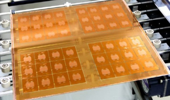
A Custom Glass Class Package Substrate is a type of advanced packaging substrate that utilizes glass as the primary material instead of traditional organic substrates or copper-clad laminates. Glass package substrates offer superior dimensional stability, excellent electrical performance, and high precision, making them ideal for applications that require ultra-fine line/space features.
In comparison to organic substrates, glass substrates provide lower dielectric loss, enabling better signal integrity at higher frequencies. Unlike copper-clad laminates, glass substrates exhibit a coefficient of thermal expansion (CTE) that closely matches silicon chips, reducing the risk of thermal stress and warping.
As semiconductor devices evolve with higher integration and smaller geometries, glass substrate solutions are gaining traction due to their ability to meet the increasing demands of 5G, high-performance computing (HPC), and AI/ML applications. Their unique advantages position them as a promising alternative in the future of advanced semiconductor packaging.
Why Choose Custom Glass Class Package Substrate?
A Custom Glass Class Package Substrate offers several advantages over traditional organic substrates and copper-clad laminates, making it an ideal choice for advanced semiconductor packaging. Below are the key reasons why glass substrates are increasingly preferred in high-performance applications.
High Precision and Ultra-Thin Characteristics
One of the main advantages of a Custom Glass Class Package Substrate is its ability to support ultra-fine line/space patterns and higher routing density. Glass substrates allow for the creation of microvias and ultra-small interconnects, enabling more compact designs and higher integration levels. This precision makes them ideal for high-frequency and miniaturized devices such as 5G communication systems and advanced AI/ML chips. Additionally, the ultra-thin nature of glass substrates contributes to reducing overall package thickness, which is crucial for modern, space-constrained applications.
Coefficient of Thermal Expansion (CTE) Matching
A significant benefit of glass substrates is their superior CTE matching with silicon chips. Unlike organic substrates, glass has a CTE that closely matches that of silicon, minimizing the risk of warping and reducing stress-induced failures during thermal cycling. This CTE compatibility enhances the reliability of the package, making it suitable for high-performance computing (HPC) and other thermally sensitive applications.
Superior Electrical Performance
The electrical properties of a Custom Glass Class Package Substrate also outperform those of organic and copper-clad substrates. Glass substrates exhibit low dielectric loss, ensuring minimal signal attenuation and high signal integrity, even in high-frequency communication environments. Additionally, their low latency characteristics make them ideal for applications requiring fast data transmission, such as high-speed networking and photonic packaging. This superior electrical performance contributes to the overall efficiency and reliability of the semiconductor package.
Types of Glass Substrates and Materials Used in Custom Glass Class Package Substrate
A Custom Glass Class Package Substrate can be manufactured using various types of glass materials, each offering unique properties that make them suitable for different advanced packaging applications. The selection of the appropriate glass material depends on the specific requirements of the application, including thermal stability, dielectric properties, and chemical resistance. Below are the primary types of glass materials used in the manufacturing of these substrates.
Borosilicate Glass for Custom Glass Class Package Substrate Applications
Borosilicate glass is a commonly used material due to its high stability and excellent chemical resistance. Known for its low thermal expansion, it is ideal for high-precision applications that require dimensional stability across a wide temperature range. This glass is also highly resistant to chemical corrosion, ensuring the substrate remains stable and reliable in harsh environments. As a result, it is frequently used in MEMS packaging, photonic devices, and high-performance computing, where long-term durability is essential.
Quartz Glass in Custom Glass Class Package Substrate Applications
Quartz glass, also known as fused silica, is another popular choice for Custom Glass Class Package Substrate due to its exceptional electrical and mechanical properties. It exhibits low dielectric loss, making it ideal for 5G and millimeter-wave (mmWave) applications where maintaining signal integrity is critical. Quartz glass also offers high mechanical strength and excellent thermal stability, allowing it to withstand extreme operating conditions without degradation. Its ability to provide low signal attenuation makes it a preferred material for high-frequency communication systems and photonic packaging.
Other Glass Types for Custom Glass Class Package Substrate Applications
In addition to borosilicate and quartz glass, other specialized materials are also used in Custom Glass Class Package Substrate production to meet specific application needs. Aluminosilicate glass, for instance, provides higher mechanical strength and impact resistance, making it suitable for applications requiring robust performance. Soda lime glass, while more cost-effective, offers good optical clarity and moderate chemical resistance, making it a viable option for less demanding applications. These alternative glass types allow manufacturers to tailor the properties of the substrate to meet the unique requirements of various semiconductor packaging technologies.
Key Application Areas for Custom Glass Class Package Substrate
A Custom Glass Class Package Substrate plays a crucial role in enhancing the performance and reliability of advanced semiconductor devices. Due to its superior electrical, thermal, and mechanical properties, glass package substrates are increasingly being adopted in a wide range of applications, including high-performance computing, 5G communication systems, advanced MEMS packaging, and photonic devices. Below are the key application areas where glass package substrates are making a significant impact.
High-Performance Computing (HPC) and AI/ML Chips
In the era of high-performance computing (HPC) and artificial intelligence/machine learning (AI/ML), multi-chip integration is essential to meet the increasing computational demands. A Custom Glass Class Package Substrate addresses the challenges associated with integrating multiple dies by offering finer line/space capabilities and improved routing density. Its superior thermal management properties help dissipate heat more effectively, reducing the risk of thermal-induced failures. Additionally, the substrate’s high dimensional stability ensures reliable operation of HPC and AI/ML chips, enhancing overall performance and longevity.
5G and Millimeter-Wave Communication Systems
The deployment of 5G and millimeter-wave (mmWave) communication systems requires substrates that can support high-frequency signals with minimal loss. A Custom Glass Class Package Substrate provides superior signal transmission due to its low dielectric constant and low signal attenuation. This enables better signal integrity and reduces electromagnetic interference, making it ideal for 5G base stations, mmWave antennas, and other high-frequency communication devices. The low-loss characteristics of glass substrates ensure that data transmission remains fast and reliable, even in demanding wireless environments.
Advanced MEMS and Sensor Packaging
Micro-electromechanical systems (MEMS) and sensor technologies require substrates that offer high sensitivity and signal reliability. Glass substrates provide a stable and inert platform that supports the integration of MEMS devices, ensuring consistent performance over time. They also facilitate the creation of microchannels, cavities, and through-glass vias (TGVs), which are essential for the packaging of MEMS and sensor devices. With a low coefficient of thermal expansion (CTE), these substrates ensure compatibility with silicon-based MEMS, reducing the likelihood of mechanical stress and enhancing overall package stability.
Photonic Packaging
Photonic devices, such as optical transceivers and silicon photonics, require substrates that offer low optical loss and high-precision alignment for high-speed data communication. A Custom Glass Class Package Substrate excels in photonic packaging by providing excellent transparency, allowing for efficient light transmission and minimizing signal loss. Its high dimensional accuracy ensures precise alignment of optical components, which is critical for maintaining the integrity of high-speed optical signals. As photonic technologies continue to advance, glass substrates are becoming an essential component in enabling next-generation photonic systems.
Manufacturing Process of Custom Glass Class Package Substrate
The manufacturing process of a Custom Glass Class Package Substrate involves multiple precision steps to ensure high performance, reliability, and scalability. This process combines advanced glass processing techniques, thin-film deposition, micro-patterning, and surface treatment to create substrates that meet the stringent requirements of high-frequency, high-density applications. Below is a detailed breakdown of the key steps involved in its production.
Precision Glass Processing
The initial stage of manufacturing a glass package substrate involves precision glass processing, where raw glass materials are treated to meet specific thickness and mechanical requirements. This process includes:
- Chemical Strengthening and Thinning: The glass substrate undergoes a chemical strengthening process, typically through ion exchange, to improve its mechanical durability and resistance to thermal stress. Thinning techniques, such as chemical etching and polishing, are used to achieve ultra-thin substrates with uniform thickness.
- Micro-Hole Processing and Laser Drilling: To create through-glass vias (TGVs) and microvias, high-precision laser drilling and mechanical CNC cutting are employed. These processes allow for the formation of ultra-small holes with high aspect ratios, enabling higher routing density and improved interconnect performance.
Thin-Film Deposition and Metallization
Once the glass substrate is prepared, the next step in creating a Custom Glass Class Package Substrate is thin-film deposition and metallization. This stage involves:
- Deposition of Cu/Al/Ag Layers: Thin films of conductive materials such as copper (Cu), aluminum (Al), and silver (Ag) are deposited on the glass substrate using techniques like sputtering and electroplating. These layers form the basis for electrical connections within the package.
- Formation of Low-Impedance Interconnects: To ensure minimal signal loss and optimal electrical performance, low-impedance interconnects are formed using precision lithography and etching techniques. This enables the creation of high-density routing and reliable connections between the chip and the substrate.
Micro-Patterning and Lithography
Micro-patterning is a critical step in defining the fine-line circuitry and via arrays on a Custom Glass Class Package Substrate. This process involves:
- Fine Patterning of Routing and Via Arrays: Advanced photolithography is used to create intricate patterns with ultra-fine line/space features, allowing for higher routing density and enhanced electrical performance.
- Alignment of Microvias and TGVs: Accurate alignment of microvias and through-glass vias (TGVs) is ensured during this stage to maintain signal integrity and reduce electrical resistance.
Surface Treatment and Final Testing
The final stage in the production of a Custom Glass Class Package Substrate involves surface treatment and quality testing to ensure long-term reliability and performance. This stage includes:
- Surface Passivation and Protection Coating: A passivation layer is applied to the surface of the substrate to protect it from environmental factors such as moisture, chemicals, and mechanical stress.
- Final Inspection and Electrical Testing: Rigorous quality control tests, including electrical characterization and mechanical durability assessments, are conducted to ensure that the substrate meets the required performance standards.
By following this comprehensive manufacturing process, the substrate achieves the high precision, electrical performance, and reliability required for cutting-edge semiconductor packaging applications.
Glass Substrates vs. Traditional Substrates: Pros and Cons of Custom Glass Class Package Substrate
As the demand for higher performance and miniaturized semiconductor devices increases, glass package substrates are emerging as a strong alternative to traditional organic substrates and copper-clad laminates (CCLs). While glass substrates offer several significant advantages, they also present certain challenges that must be addressed for widespread adoption. Below is a detailed comparison of the pros and cons of a Custom Glass Class Package Substrate.
Advantages of Glass Substrates
Glass substrates provide numerous advantages over traditional organic and copper-based substrates, making them ideal for advanced semiconductor packaging.
-
Better Mechanical Stability
A Custom Glass Class Package Substrate offers exceptional mechanical stability due to the inherent properties of glass. Unlike organic substrates, glass exhibits minimal warping and deformation under high temperatures, ensuring dimensional accuracy and reliability during thermal cycling. This makes glass substrates highly suitable for applications where consistent mechanical performance is critical, such as high-performance computing (HPC) and artificial intelligence/machine learning (AI/ML) chips. -
Enhanced Electrical Properties
One of the key advantages of a Custom Glass Class Package Substrate is its superior electrical performance. Glass has a lower dielectric constant and minimal signal loss, allowing for higher signal integrity and reduced electromagnetic interference (EMI). These properties make glass substrates ideal for high-frequency applications, such as 5G/mmWave communication systems and photonic devices. Additionally, the lower dielectric loss of glass substrates contributes to faster data transmission and improved overall package performance. -
Improved Thermal Management
The low coefficient of thermal expansion (CTE) of glass matches closely with that of silicon, reducing the risk of thermal-induced stress and enhancing package reliability. This property is particularly beneficial for multi-chip modules (MCMs) and heterogeneous integration scenarios where thermal mismatches can lead to performance degradation.
Challenges of Glass Substrates
Despite the many advantages of a Custom Glass Class Package Substrate, certain challenges must be addressed before it can replace traditional substrates in large-scale production.
-
Higher Manufacturing Costs
One of the primary challenges associated with a Custom Glass Class Package Substrate is the higher manufacturing cost compared to traditional organic substrates and copper-clad laminates. The precision required in glass processing, including chemical strengthening, laser drilling, and micro-patterning, adds to the overall cost of production. Additionally, the use of specialized equipment and materials further increases the cost per unit, making glass substrates less cost-effective for low-margin applications. -
Need for Precision Fabrication Technology
The production of a Custom Glass Class Package Substrate requires extremely precise fabrication technologies to achieve the desired level of accuracy and performance. Processes such as micro-hole drilling, through-glass via (TGV) formation, and metallization must be carried out with high precision to maintain signal integrity and mechanical stability. Any deviation during fabrication can result in defects that compromise the performance of the entire package. -
Integration Challenges
Integrating glass substrates into existing packaging workflows may require modifications to current assembly and testing processes. As glass substrates have different handling and bonding requirements compared to organic substrates, manufacturers may need to invest in new equipment and develop specialized assembly techniques to ensure seamless integration.
While glass substrates offer remarkable advantages in mechanical stability, electrical performance, and thermal management, overcoming the challenges related to manufacturing costs and precision fabrication remains essential for broader adoption. As fabrication technologies continue to advance and production costs decrease, these substrates are poised to become a key enabler in the future of semiconductor packaging.
Market Trends and Industry Insights for Custom Glass Class Package Substrate
As the semiconductor industry pushes the boundaries of performance, miniaturization, and high-frequency applications, glass substrates are gaining significant traction. They are emerging as a viable alternative to organic substrates and copper-clad laminates (CCLs) in advanced packaging due to their superior electrical, thermal, and mechanical properties. The adoption of glass substrates is driven by key industry players and ongoing technological innovations that are shaping the future of semiconductor packaging.
Key Industry Players and Latest Developments
Several major manufacturers are at the forefront of developing and commercializing Custom Glass Class Package Substrate technologies, contributing to rapid advancements in glass substrate applications.
-
AGC Inc.
AGC, a leading global glass manufacturer, is pioneering the development of advanced glass substrates for semiconductor packaging. Its proprietary SWAN™ (Smart Wafer and Advanced Glass for Next-gen devices) technology offers high-precision glass substrates with ultra-low warpage and fine-pitch interconnections, making them ideal for 5G, AI, and high-performance computing (HPC) applications. -
Schott AG
Schott, a global leader in specialty glass manufacturing, is actively driving innovations in Custom Glass Class Package Substrate solutions. The company’s Nexterion® glass substrates provide superior optical clarity and mechanical stability, making them suitable for advanced MEMS and photonic packaging. Schott’s expertise in precision glass processing positions it as a key player in enabling next-generation semiconductor packaging technologies. -
Nexterion (Schott’s Brand for Glass Substrates)
Nexterion offers a wide range of high-performance glass substrates specifically designed for semiconductor and MEMS applications. Its products feature excellent surface quality, low dielectric loss, and high dimensional accuracy, making them an excellent choice for Custom Glass Class Package Substrate applications. -
SusteelGlass
SusteelGlass, a rising player in the glass substrate industry, specializes in providing custom glass wafers and substrates for semiconductor and microelectronics applications. Their advanced fabrication techniques enable the production of ultra-thin glass substrates with high precision, catering to the evolving demands of the semiconductor industry. -
Other Key Players
Other industry leaders, including Corning, Terra Universal, and Alcanta PCB, are also making significant strides in developing innovative Custom Glass Class Package Substrate solutions. These companies are investing heavily in research and development to enhance glass substrate performance and reduce manufacturing costs, accelerating the adoption of glass substrates in advanced packaging.
Technological Innovations and Future Prospects
The evolution of Custom Glass Class Package Substrate technology is being driven by several disruptive innovations and emerging trends that are poised to reshape the semiconductor packaging landscape.
-
Glass Core Substrate (GCS) as a Disruptive Technology
One of the most notable advancements in the field of glass substrates is the development of Glass Core Substrate (GCS) technology. GCS utilizes ultra-thin glass as the core layer of the package substrate, enabling higher routing density, lower signal loss, and improved thermal management. This innovative approach enhances the performance of high-bandwidth devices, including 5G transceivers, AI accelerators, and photonic integrated circuits. As GCS technology matures, it is expected to become a game-changer in the semiconductor industry, driving widespread adoption of Custom Glass Class Package Substrate solutions. -
Adoption of Glass Substrates in Advanced Packaging Applications
As semiconductor devices continue to shrink and become more complex, the need for advanced packaging technologies that can support higher integration levels and faster data transmission is increasing. Custom Glass Class Package Substrate solutions are finding their way into various advanced packaging applications, including:- Fan-Out Wafer-Level Packaging (FO-WLP): Glass substrates provide better thermal stability and mechanical strength, making them ideal for FO-WLP designs that require high-density interconnects.
- 2.5D and 3D Integration: The use of glass substrates in 2.5D and 3D packaging enhances signal integrity and enables higher data rates, paving the way for next-generation high-performance systems.
- Heterogeneous Integration and Chiplet Architectures: Glass substrates support the seamless integration of multiple chiplets with different functionalities, enabling heterogeneous integration that enhances overall system performance.
-
Future Prospects and Market Growth
The market for Custom Glass Class Package Substrate solutions is expected to experience rapid growth over the next decade, driven by increasing demand for high-frequency, high-speed, and miniaturized semiconductor devices. As manufacturing technologies advance and production costs decrease, glass substrates are likely to replace traditional organic substrates in many high-performance applications. Additionally, the emergence of glass-based interposers and fan-out packages is expected to further accelerate the adoption of glass substrates in advanced packaging.
The growing involvement of key industry players and the continuous development of disruptive technologies position glass substrate solutions as a critical enabler for the future of semiconductor packaging. As these substrates become more cost-effective and scalable, they are expected to play a pivotal role in driving the next wave of innovation in the semiconductor industry.
Future Outlook: Can Custom Glass Class Package Substrate Replace Traditional Substrates?
As the demand for higher performance, miniaturization, and improved thermal management continues to grow, glass-based solutions are increasingly being considered as a viable alternative to traditional organic substrates and copper-clad laminates (CCLs). However, for glass substrates to fully replace traditional options, significant advancements in technology, cost reduction, and scalability are required. Below is a comprehensive outlook on the future prospects of glass substrates and their potential to reshape the semiconductor packaging industry.
Technological Breakthroughs and Cost Reduction
To make Custom Glass Class Package Substrate a mainstream solution, technological breakthroughs and cost reduction are essential. Currently, the high cost of glass substrates is one of the biggest barriers to widespread adoption. However, ongoing research and development efforts are focused on optimizing manufacturing processes and improving yield rates to lower production costs.
- Innovations in Through-Glass Via (TGV) Formation: Advances in laser drilling, chemical etching, and precision CNC machining are making it possible to create ultra-small TGVs with higher aspect ratios, enabling higher routing density and improved signal integrity. As TGV formation technologies continue to mature, they will contribute to reducing fabrication costs and increasing yield rates.
- Enhanced Metallization Techniques: The development of improved metallization techniques, such as electroplating and sputtering for Cu/Al/Ag layers, is enhancing the reliability of interconnects while minimizing signal loss. These advancements will enable more cost-effective production of Custom Glass Class Package Substrate solutions with superior electrical performance.
- Cost-Effective Thin Glass Processing: Chemical thinning and polishing techniques are being optimized to produce ultra-thin glass substrates at lower costs. Additionally, the use of alternative materials such as soda-lime glass and aluminosilicate glass in less demanding applications can reduce material costs while maintaining acceptable performance.
As these technological innovations gain traction, they will gradually bring down the cost of Custom Glass Class Package Substrate solutions, making them a more competitive option for a wider range of semiconductor applications.
Scalability and Mass Production Feasibility
For Custom Glass Class Package Substrate to replace traditional substrates on a larger scale, scalability and mass production feasibility are critical. While glass substrates offer superior performance in many areas, challenges related to high-volume manufacturing and integration into existing semiconductor workflows must be addressed.
- Automation and High-Throughput Processing: Developing high-throughput manufacturing systems that can handle precision glass processing at scale is key to reducing production costs and increasing efficiency. Automated handling and alignment systems will enable faster production times and higher yield rates, making glass substrates more commercially viable.
- Standardization of Glass Substrate Designs: Establishing industry standards for Custom Glass Class Package Substrate designs, including via sizes, metallization patterns, and bonding processes, will facilitate mass adoption and seamless integration into semiconductor packaging workflows. Standardization will also reduce design complexity and streamline the supply chain, making it easier for manufacturers to transition to glass substrates.
- Adoption of Glass Core Substrate (GCS) in High-Volume Applications: The introduction of Glass Core Substrate (GCS) technology offers a scalable solution for high-performance applications. As GCS production techniques mature and become more cost-effective, they will enable widespread adoption of glass substrates in high-volume markets, such as 5G, AI, and high-performance computing.
Industry Forecast for the Next 3-5 Years
Over the next 3-5 years, the market for Custom Glass Class Package Substrate is expected to grow significantly as technological advancements and cost reductions make glass substrates a more attractive option for semiconductor packaging.
- Increased Adoption in High-Performance Applications: Glass substrates will see higher adoption in high-frequency, high-bandwidth applications such as 5G/mmWave communication systems, photonics, and AI/ML accelerators. Their ability to offer superior signal integrity and thermal management will drive demand in these sectors.
- Expansion of Glass-Based Packaging Technologies: The introduction of glass-based interposers, fan-out packages, and heterogeneous integration platforms will further accelerate the adoption of Custom Glass Class Package Substrate solutions. As the industry shifts toward multi-chip integration and 3D packaging, glass substrates will play a key role in enabling next-generation semiconductor designs.
- Shift Toward Cost-Effective Manufacturing Models: With ongoing process improvements and the introduction of scalable production techniques, the cost of glass substrates is expected to decrease, making them more accessible for mainstream semiconductor applications. This will lead to broader adoption across multiple industries and drive the overall growth of the glass substrate market.
While glass substrates are currently positioned as a premium option for high-performance applications, rapid advancements in technology, cost optimization, and scalability are paving the way for broader adoption. As the industry continues to innovate and address manufacturing challenges, these substrates are poised to become a key enabler in the future of semiconductor packaging, potentially replacing traditional options in many high-performance applications.