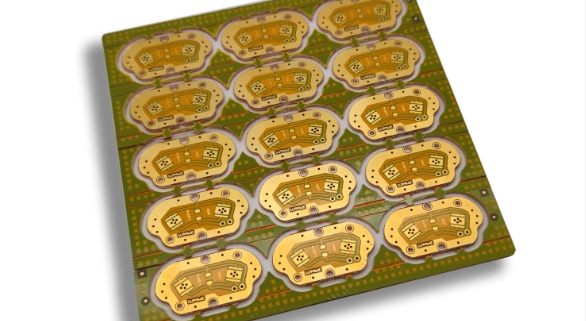
Welcome to our exploration of FR-1 PCB substrate! In the world of printed circuit boards (PCBs), selecting the appropriate substrate material is paramount for ensuring performance, reliability, and safety. As such, understanding the characteristics and applications of different substrate materials is crucial. In this blog, we will delve into FR-1 material, shedding light on its composition, properties, and advantages in PCB manufacturing. We’ll also compare it to other common materials like FR-4, and discuss the significance of FR materials in general. By the end, you’ll have a comprehensive understanding of FR-1 PCB substrate and its role in electronic design and fabrication. Let’s dive in!
阅读更多Clear PCB substrate refers to the use of transparent materials as the base for printed circuit boards (PCBs), allowing visibility through the board. The substrate material in PCBs is crucial as it provides mechanical support and electrical insulation. However, with the emergence of transparent substrates, PCBs have entered a new realm of innovation. This blog aims to delve into the significance of substrate materials in PCBs, particularly focusing on transparent options. By exploring the advantages, applications, and manufacturing processes of clear PCBs, readers will gain insights into the future of PCB technology and its potential impact across various industries.
阅读更多Printed Circuit Boards (PCBs) serve as the backbone of modern electronics, providing the structural and electrical framework for electronic components. PCB substrates, the base material upon which circuits are built, play a crucial role in determining the performance and reliability of electronic devices. Among various substrate options, ceramic PCB substrates have gained prominence for their exceptional properties and performance. Unlike traditional FR-4 substrates, which are composed of fiberglass and epoxy resin, ceramic substrates utilize ceramic materials such as alumina or aluminum nitride. In this blog, we delve into the unique features and advantages of ceramic PCB substrates, exploring their suitability for diverse electronic applications.
阅读更多Printed Circuit Boards (PCBs) serve as the backbone of modern electronics, facilitating the interconnection of electronic components and enabling the functionality of a vast array of devices. Their significance in the realm of technology cannot be overstated, as they are integral to everything from smartphones to spacecraft.
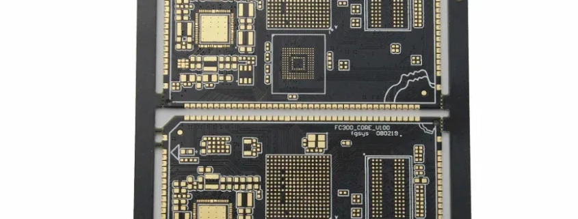
In this article, we delve into a specific aspect of PCBs: the emergence and utilization of black PCB substrates. While traditional green PCBs have long dominated the industry, black PCBs are gaining traction for their distinct aesthetics and functional advantages. Throughout this discussion, we’ll explore the characteristics, applications, manufacturing processes, costs, and future trends associated with black PCB substrates, shedding light on their growing relevance in electronic design and manufacturing.
阅读更多Printed Circuit Board (PCB) serves as the backbone of modern electronics, facilitating the connection and integration of electronic components. PCBs provide a platform for the assembly of intricate circuits in a compact and efficient manner. The term “PCB” refers to a board made of insulating material, typically fiberglass-reinforced epoxy, with conductive pathways etched or printed onto its surface. These pathways allow for the flow of electrical signals between components. The selection of the right PCB substrate is paramount as it directly impacts the performance, reliability, and longevity of electronic devices. Choosing an appropriate substrate material ensures optimal electrical properties, thermal management, and mechanical stability, thus enhancing the overall functionality and durability of electronic systems.
阅读更多PCB substrates are the foundational materials of printed circuit boards, providing structural support and insulation for electronic circuits. Their role is critical in determining the performance, durability, and thermal management of the PCB. A PCB substrate is the base layer made from insulating materials that support electronic components, ensure electrical insulation, and facilitate heat dissipation. This is essential for the reliability and longevity of electronic devices.
Aluminum PCB substrates consist of an aluminum base, a dielectric insulating layer, and a copper conductive layer. Known for their excellent thermal conductivity, aluminum PCBs efficiently dissipate heat from components, making them ideal for high-power and high-temperature applications. Key benefits of aluminum PCB substrates include superior heat dissipation, mechanical stability, and cost-effectiveness. They are extensively used in LED lighting, power electronics, automotive systems, and consumer electronics, where effective heat management is vital. These advantages make aluminum PCBs a popular choice in modern electronics.
阅读更多Printed Circuit Boards (PCBs) serve as the backbone of modern electronic devices, providing a platform for interconnecting electronic components. The choice of PCB substrate material significantly impacts the performance, reliability, and functionality of these devices. Among the array of substrate options available, alumina PCB substrates stand out for their exceptional properties and versatility.
Alumina, also known as aluminum oxide (Al2O3), emerges as a preferred substrate material due to its unique combination of high thermal conductivity, electrical insulation, and mechanical robustness. This makes alumina PCB substrates well-suited for a diverse range of applications spanning industries such as aerospace, automotive, telecommunications, and consumer electronics. In this blog, we delve deeper into the features, advantages, and applications of alumina PCB substrates, exploring how they contribute to the advancement of electronic device manufacturing and innovation.
阅读更多Printed Circuit Boards (PCBs) serve as the backbone of modern electronic devices, facilitating the interconnection of components through conductive pathways. The fabrication and assembly process involves intricate stages of designing, etching, and soldering, ensuring precise execution to meet functional requirements. However, even with meticulous manufacturing, defects may occur, underscoring the critical role of electrical testing. Electrical testing serves as the final checkpoint, verifying the integrity and functionality of PCBs before deployment. Among various PCB configurations, 4-layer PCB substrates stand out for their versatility, accommodating complex circuitry while maintaining compact form factors. Understanding their significance is crucial, as they underpin the performance of diverse electronic applications, from consumer electronics to aerospace systems.
阅读更多QFN (Quad Flat No-Lead) packaging is a type of surface-mount integrated circuit package characterized by a flat bottom surface with no leads extending from the body. Its design enables direct soldering onto the PCB, reducing the footprint and enhancing thermal and electrical performance. Originally introduced in the late 1990s, QFN packages have gained widespread adoption across various electronic devices, including smartphones, computers, and automotive electronics, due to their compact size, improved heat dissipation, and excellent electrical properties. This packaging format facilitates higher component density on PCBs, contributing to miniaturization and improved functionality in modern electronic designs.
阅读更多Semiconductor packaging plays a crucial role in protecting integrated circuits and facilitating their integration into electronic systems. Among the various packaging options, the Quad Flat No-leads (QFN) package has gained significant traction in recent years. QFN packaging offers a compact and reliable solution for mounting integrated circuits onto printed circuit boards (PCBs). Unlike traditional leaded packages, QFN packages feature no external leads, maximizing space efficiency and enhancing electrical performance. In this blog, we delve deeper into the world of QFN packaging, exploring its types, advantages, disadvantages, and the specific innovation of the open cavity QFN package.
阅读更多CONTACT US
4th Floor, A3 Building, HuaFeng Industrial Park, GuanTian Village, BeiHuan Road, ShiYan Street, Bao An District, Shenzhen City, Guangdong Province, China
Tel:086 (0)755-8524-1496
WhatsApp: 8615014077679
Skype: Henrychinasz
📧 pcb@alcantapcb.com
CONTACT US
SHIPPING
CERTIFCATION
recent articles
- Understanding Multilayer Substrate Technology in Electronics2024-12-26 - 3:11 上午
- Types of Material Substrate and Their Diverse Applications2024-12-25 - 2:13 上午
- Real-World Applications of LTCC Multilayer Substrate in Technology2024-12-24 - 3:34 上午
- Understanding Leadframe vs Substrate: Roles in Packaging2024-12-23 - 3:56 上午