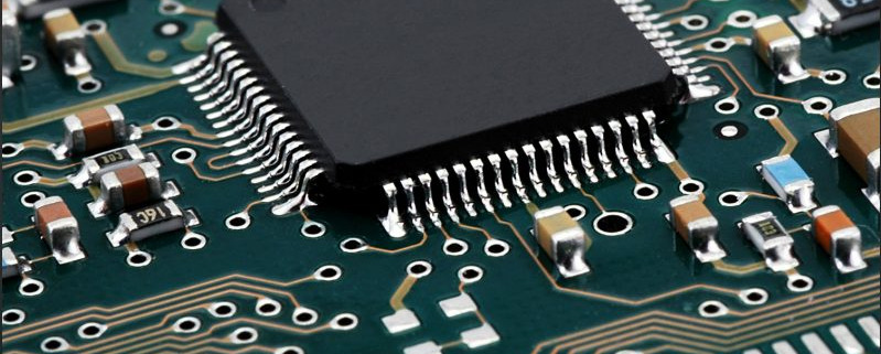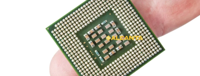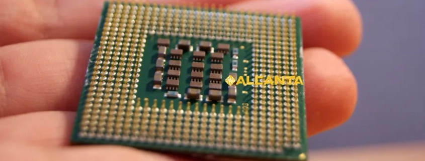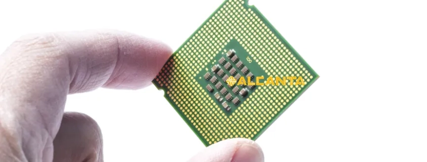
Printed Circuit Boards (PCBs) are essential components in modern electronic devices, providing a platform to mechanically support and electrically connect electronic components using conductive pathways, or traces, etched from copper sheets laminated onto a non-conductive substrate. PCBs are found in virtually all electronic devices, from simple gadgets to complex computing systems.
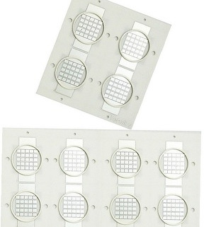
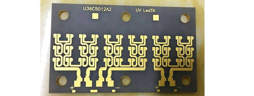
Ceramic substrate PCBs, a specialized type of PCB, use ceramic materials such as alumina, aluminum nitride, or silicon nitride as the base. These substrates offer superior thermal conductivity, mechanical strength, and electrical insulation compared to traditional materials like FR-4 (a composite of woven glass fabric and epoxy resin). Due to their exceptional properties, ceramic substrate PCB are crucial in high-power, high-frequency, and high-reliability applications. They are commonly used in aerospace, automotive electronics, medical devices, and communication equipment, where performance and durability are paramount. The unique advantages of ceramic substrates make them indispensable in advancing technology in these critical fields.
阅读更多