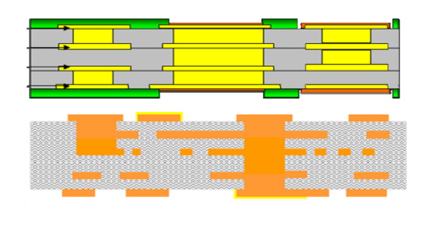
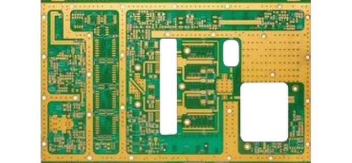
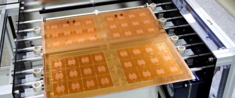
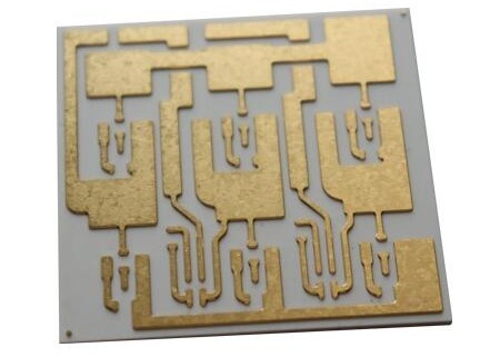
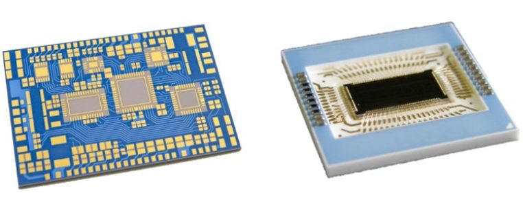
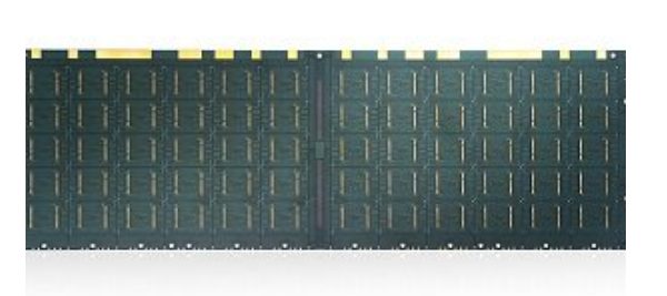
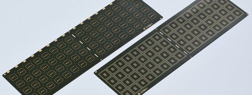
Leadframe substrates are critical components in the semiconductor industry, serving as the foundation for various packaging solutions. Their primary role is to connect the semiconductor die to external circuits, ensuring reliable electrical performance and mechanical stability. As technology advances, the demand for compact, efficient, and high-performance electronic devices increases, making leadframe substrates essential for meeting these requirements. This article will delve into the definition and functions of leadframes, explore the differences between leadframes and laminate substrates, and highlight the significance of companies like Amkor and packaging types such as QFP. Additionally, we will examine the raw materials used in leadframe manufacturing and their applications in semiconductor packaging. By understanding these aspects, readers will gain insight into the pivotal role leadframe substrates play in the evolving landscape of electronic technology.
阅读更多Semiconductor packaging is a crucial aspect of electronic device manufacturing, as it protects sensitive components and ensures reliable electrical connections. Proper packaging enhances performance, thermal management, and durability, playing a significant role in the overall functionality of integrated circuits (ICs). Among various packaging methods, Lead Frames and Substrates are two widely used components.
Lead Frames serve as conductive pathways that connect the semiconductor chip to external circuitry, providing mechanical support and facilitating electrical signals. They are typically made from metal and are essential in traditional package types like dual in-line packages (DIPs).
On the other hand, Substrates offer a platform for mounting chips, incorporating additional circuitry and thermal dissipation features. They come in various forms, including IC Substrates and Package Substrates, each designed to meet specific performance requirements. Understanding the distinctions and applications of Lead Frames and Substrates is vital for optimizing semiconductor packaging solutions.
阅读更多In the rapidly evolving world of modern electronics, substrates serve as the unsung heroes, underpinning the functionality and reliability of countless devices. From smartphones to sophisticated computing systems, the quality and performance of substrates directly influence the efficiency and durability of these gadgets. Substrates play a pivotal role in semiconductor and PCB manufacturing, acting as the foundational layer that supports and connects various electronic components. Without these crucial elements, the seamless operation of integrated circuits and printed circuit boards would be impossible.
This article aims to shed light on the intricate processes involved in substrate manufacturing. By diving deep into the methodologies and materials used, we will differentiate IC substrates from PCBs, highlighting their unique properties and applications. Whether you are an industry professional or an electronics enthusiast, this comprehensive guide will equip you with valuable insights into the world of substrate technology.
阅读更多Substrates are the foundational materials upon which electronic circuits and components are built, playing a crucial role in the functionality and reliability of electronic devices. They provide the necessary support for the assembly of electronic components, ensuring electrical insulation, heat dissipation, and mechanical stability. In essence, the quality and characteristics of substrates significantly influence the performance and durability of electronic products ranging from everyday gadgets to complex computing systems.
The substrate manufacturing industry is a vital segment of the electronics supply chain. It encompasses a variety of processes and technologies to produce substrates tailored for different applications, such as printed circuit boards (PCBs), integrated circuits (ICs), and semiconductor devices. This industry is driven by continuous advancements in materials science and manufacturing techniques, aiming to meet the increasing demands for miniaturization, higher performance, and cost-effectiveness in electronics. Key players in this industry are constantly innovating to develop substrates with superior properties, catering to the evolving needs of various high-tech sectors.
阅读更多Laminate materials are composed of multiple layers bonded together to create a durable, lightweight, and versatile substrate. They play a crucial role in packaging by providing enhanced protection, improved structural integrity, and customizable properties tailored to specific needs. Their applications span various industries, from food packaging to electronics, making them indispensable in modern manufacturing.
In this article, we will focus on the application of laminate substrates in semiconductor packaging. These substrates are essential for supporting and protecting delicate semiconductor components, ensuring optimal performance and reliability. By exploring their unique characteristics and benefits, we aim to highlight the significance of laminate substrates in advancing semiconductor technology and their contribution to the growing demand for efficient packaging solutions.
阅读更多Laminate substrates play a crucial role in modern technology, serving as essential components in various industries. Their lightweight, durable nature and excellent electrical insulation properties make them ideal for applications in electronics, where they are widely used in printed circuit boards (PCBs). In the aerospace sector, laminate substrates are valued for their high thermal stability and resistance to harsh environments, ensuring reliable performance in critical systems. Similarly, the automotive industry benefits from their ability to withstand temperature fluctuations and mechanical stress, enhancing the durability of electronic components within vehicles. As the demand for more advanced and compact technologies grows, laminate substrates continue to be at the forefront, driving innovation and efficiency across multiple sectors. Their versatility and reliability make them indispensable in creating high-performance products that meet the stringent requirements of today’s applications.
阅读更多Kyocera Corporation, headquartered in Kyoto, Japan, plays a pivotal role in the global electronics industry. Known for its advanced ceramic technology, Kyocera manufactures a diverse range of products including electronic components, industrial tools, and equipment for telecommunications and automotive sectors. With operations spanning across Asia, Americas, Europe, and beyond, Kyocera boasts extensive market coverage, delivering innovative solutions that cater to high-tech industries worldwide. The company’s commitment to quality and sustainability underscores its leadership in providing reliable components essential for modern electronic applications.
Kyocera Build-up Substrates
Definition and Applications of Build-up Substrates
Build-up substrates are advanced PCBs designed with multiple layers of insulating and conductive materials. They enable complex circuitry and miniaturization in electronic devices, supporting high-density interconnects (HDI) and fine pitch components. Kyocera’s build-up substrates integrate precision manufacturing techniques to achieve tight tolerances and reliability in signal transmission and power distribution.
Kyocera’s Technological and Product Advantages in Build-up Substrates
Kyocera excels in build-up substrate technology through its expertise in ceramic materials and microfabrication. Their substrates feature low-loss dielectrics, high thermal conductivity, and excellent mechanical stability, crucial for demanding applications in telecommunications, aerospace, and medical devices. Kyocera’s innovations include customizable designs, ensuring optimal performance in diverse electronic environments.
Real-world Applications and Case Studies
Kyocera’s build-up substrates are integral to smartphones, automotive electronics, and IoT devices. For example, in automotive electronics, they enhance reliability and performance in control modules and infotainment systems. Case studies highlight their role in enabling compact, high-performance solutions that meet stringent industry standards and deliver exceptional reliability in challenging operational environments.
Kyocera Multilayer Ceramic Capacitors (MLCCs)
Basic Principles and Structure of MLCCs
MLCCs are passive electronic components composed of alternating layers of ceramic materials and metal electrodes. They store electrical energy and filter out high-frequency noise in circuits. Kyocera’s MLCCs utilize advanced ceramic formulations and precise layering techniques to achieve high capacitance densities and stable performance across a wide range of temperatures and frequencies.
Kyocera’s Expertise and Technological Advantages in Manufacturing MLCCs
Kyocera leads in MLCC manufacturing due to its deep expertise in ceramic materials and process innovation. Their MLCCs feature low equivalent series resistance (ESR), high reliability, and excellent temperature stability, crucial for applications in consumer electronics, automotive systems, and industrial equipment. Kyocera’s proprietary manufacturing techniques ensure consistent quality and support customization to meet specific customer requirements.
Applications and Market Demand for MLCCs in Electronic Products
MLCCs are essential in smartphones, computers, power supplies, and IoT devices, where they support miniaturization and enhance circuit performance. The market demand for MLCCs continues to grow, driven by increasing electronic device complexity and the need for compact, efficient components. Kyocera’s MLCCs address these demands with robust designs that ensure optimal electrical performance and reliability in diverse applications.
Kyocera Industrial Tools Corporation
Business Scope and Product Types of Kyocera Industrial Tools Corporation
Kyocera Industrial Tools Corporation specializes in providing cutting tools and solutions for various industries, including automotive, aerospace, and electronics manufacturing. Their product range includes precision cutting tools, indexable inserts, and tool holders designed to enhance machining efficiency, accuracy, and tool life. Kyocera’s tools are renowned for their high-performance materials and advanced coatings, which optimize cutting processes in challenging manufacturing environments.
Support Provided by Industrial Tools Corporation in Electronic Manufacturing and Assembly Processes
In electronic manufacturing, Kyocera Industrial Tools Corporation plays a crucial role by offering specialized tools for PCB fabrication, such as drills, end mills, and routers. These tools are essential for precision machining of substrates, ensuring accurate dimensions and surface finishes critical for circuit board assembly. Kyocera’s cutting-edge technologies and application expertise help electronic manufacturers improve throughput, reduce scrap, and maintain stringent quality standards in production lines worldwide.
Kyocera High-Temperature Ceramic Substrates
Importance and Characteristics of High-Temperature Ceramic Substrates
High-temperature ceramic substrates play a critical role in electronic applications where extreme heat resistance, thermal stability, and electrical insulation are essential. These substrates can withstand temperatures ranging from hundreds to thousands of degrees Celsius without degrading, making them ideal for harsh environments and demanding industrial processes. They offer excellent mechanical strength, low thermal expansion, and high dielectric strength, ensuring reliable performance in aerospace, automotive, and industrial applications.
Kyocera’s Ceramic Substrate Technology and Product Features for High-Temperature Electronic Integration
Kyocera excels in high-temperature ceramic substrate technology through advanced material formulations and precise manufacturing processes. Their substrates feature specialized ceramic compositions optimized for thermal conductivity and mechanical robustness. Kyocera utilizes proprietary bonding and layering techniques to create dense, uniform substrates capable of supporting high-power electronics and circuitry in extreme thermal conditions. These substrates enable compact designs and enhance the efficiency and reliability of electronic systems operating in elevated temperatures.
Application Cases in Aerospace, Automotive Electronics, and Industrial Control
Kyocera’s high-temperature ceramic substrates are integral to aerospace applications such as satellite communications, where they ensure stable performance of onboard electronics in space environments. In automotive electronics, these substrates support power modules and sensors that operate in engine compartments, withstanding thermal cycling and vibrations. In industrial control systems, they enable the reliable operation of high-power electronics in factories and power plants, enhancing equipment efficiency and longevity. Kyocera’s ceramic substrates contribute to advancing technology in critical sectors by enabling robust electronic integration under challenging thermal conditions.
FAQs about kyocera substrate
No, Kyocera is not a Chinese company. It is a Japanese multinational corporation.
The substrate used in electronic packaging can vary, but common types include FR4 (fiberglass-reinforced epoxy laminate), ceramics, and various specialized materials designed for specific applications.
A ceramic substrate is a type of base material used in electronics, made from ceramic materials that offer advantages such as high thermal conductivity, electrical insulation, and mechanical stability.
Ceramic substrates for high-temperature electronic integration are designed to withstand extreme heat conditions, providing thermal management and reliability for electronic components in aerospace, automotive, and industrial applications.
Kyocera Corporation, founded in 1959 in Japan, has grown into a global leader renowned for its innovative technologies across various sectors. In the electronics industry, Kyocera plays a pivotal role as a provider of advanced ceramic substrates and components critical for electronic devices’ performance and reliability. Leveraging decades of expertise, Kyocera’s solutions are integral to high-temperature electronic integration, offering robustness and efficiency in demanding environments. The company’s commitment to quality and sustainability underscores its reputation, driving advancements that meet evolving industry needs. Kyocera continues to shape the future of electronics through continuous innovation and steadfast dedication to technological excellence.
阅读更多An Interposer Substrate serves as a vital intermediary in integrated circuits, facilitating connections between different semiconductor components or between a semiconductor and a package substrate. Its role is crucial in enhancing performance, enabling denser integration, and managing thermal and electrical properties effectively. Interposers enable advanced packaging techniques like CoWoS (Chip-on-Wafer-on-Substrate), enabling higher bandwidth and lower power consumption in devices. They bridge the gap between heterogeneous technologies, optimizing signal integrity and reducing latency. In modern electronics, Interposer Substrates are pivotal for achieving compact, high-performance designs in applications ranging from high-speed computing to telecommunications and beyond.
阅读更多Intel Corporation stands at the forefront of the global semiconductor industry, renowned for its pioneering innovations and technological leadership. This blog aims to provide an insightful overview of Intel’s substrate products, exploring their pivotal role in the manufacturing of advanced semiconductor devices. From defining semiconductor substrates to delving into Intel’s cutting-edge chip manufacturing processes, this outline will highlight the significance of Intel’s glass substrates and TGV technology. By examining Intel’s substrate supply chain and future prospects, we aim to showcase how these components contribute to Intel’s continued dominance in shaping the future of technology.
阅读更多CONTACT US
4th Floor, A3 Building, HuaFeng Industrial Park, GuanTian Village, BeiHuan Road, ShiYan Street, Bao An District, Shenzhen City, Guangdong Province, China
Tel:086 (0)755-8524-1496
WhatsApp: 8615014077679
Skype: Henrychinasz
📧 pcb@alcantapcb.com
CONTACT US
SHIPPING
CERTIFCATION
recent articles
- Key Differences Between FR4 Rogers Double Sided PCB Materials2025-01-13 - 2:12 上午
- A Guide to FR4 PCB, Rogers PCB, and Aluminum PCB2025-01-10 - 1:38 上午
- Materials Used in Substrate for Chips and Their Advantages2025-01-09 - 2:58 上午
- Understanding Substrate Dielectric FR4: Key Properties and Uses2025-01-08 - 5:08 上午