
Key Benefits of Plastic Leaded Chip Carrier (PLCC) Lead Frame
Plastic Leaded Chip Carrier (PLCC) Lead Frame is a semiconductor packaging technology designed for efficient, reliable IC connections. This surface-mount package features J-leads, offering mechanical support and electrical connectivity in a compact form. PLCC is significant in electronics as it allows for high-density PCB designs and can be used with surface-mount technology (SMT) or in sockets for easy replacement. Its versatility makes it ideal for applications like microcontrollers, memory chips, and logic devices, requiring durability, reusability, and high thermal performance. The purpose of this article is to provide a detailed exploration of PLCC, discussing its structure, manufacturing process, advantages, and key applications in the modern electronics industry.
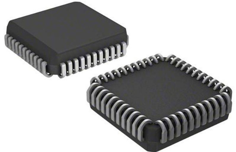
Overview of Plastic Leaded Chip Carrier (PLCC) Lead Frame Packaging
Plastic Leaded Chip Carrier (PLCC) Lead Frame is a widely used semiconductor packaging type that provides a reliable and durable solution for integrated circuits (ICs). PLCC stands for “Plastic Leaded Chip Carrier,” referring to its plastic-encased design with leaded connections. The Lead Frame, an essential component of the package, serves as the structural foundation that supports the IC and provides electrical connectivity between the chip and the printed circuit board (PCB).
Key Characteristics of PLCC Packaging
The package features a plastic-encased design that protects the internal IC from physical damage and environmental factors. It utilizes J-shaped leads that extend from the sides and fold underneath the package. This lead structure allows for both surface-mount technology (SMT) installation and insertion into dedicated sockets, providing high versatility. Additionally, its compact form factor offers a balance between density and accessibility, making it suitable for various electronic applications.
Common Applications of PLCC
Due to its durability and compatibility with different mounting methods, this lead frame is commonly used in applications requiring reliable performance and reusability. It is frequently found in microcontrollers, memory chips (such as EEPROMs and Flash memory), logic ICs, and digital signal processors. The combination of structural integrity and electrical efficiency makes it a preferred choice in industrial, automotive, and consumer electronics.
PLCC Lead Frame Structure and Design in Plastic Leaded Chip Carrier (PLCC) Lead Frame
Role of the Lead Frame in PLCC Packaging
Plastic Leaded Chip Carrier (PLCC) Lead Frame serves as the backbone of the PLCC package, providing mechanical support and electrical pathways for the integrated circuit (IC). The Lead Frame connects the internal chip to external circuitry by forming a conductive bridge between the IC and the PCB. Its design ensures structural stability, effective heat dissipation, and reliable electrical conductivity. The J-lead structure of PLCC enhances durability and allows for both surface-mount technology (SMT) and socket installation, making it adaptable for various electronic applications.
Materials Used for Lead Frames
To ensure high electrical conductivity and mechanical strength, the lead frame is primarily made from copper alloys. Copper provides excellent thermal and electrical performance, making it the preferred choice for construction. To enhance durability and prevent oxidation, the lead frame is often plated with metals such as nickel, gold, or tin.
- Nickel plating improves corrosion resistance and adhesion for subsequent layers.
- Gold plating ensures excellent conductivity and enhances wire bonding reliability.
- Tin plating prevents oxidation and facilitates soldering during PCB assembly.
Manufacturing Processes: Stamping vs. Etching
The manufacturing of Plastic Leaded Chip Carrier (PLCC) Lead Frame typically follows two main processes: stamping and etching.
- Stamping: This method involves using high-speed mechanical presses to cut and form the Lead Frame from a metal sheet. Stamping is a cost-effective, high-volume production technique that ensures precision and uniformity.
- Etching: A chemical process that removes unwanted material to create the desired Lead Frame pattern. Etching allows for intricate designs and is ideal for applications requiring fine details and minimal mechanical stress.
Both methods contribute to the efficiency and reliability of the packaging, ensuring it meets the demands of modern electronic applications.
PLCC Package Types and Dimensions in Plastic Leaded Chip Carrier (PLCC) Lead Frame
Common PLCC Sizes
PLCC is available in multiple sizes to accommodate different integrated circuit (IC) applications. The most common package sizes include:
- PLCC-20: Typically used for small logic ICs and low-pin-count microcontrollers.
- PLCC-32: Commonly found in EEPROMs, flash memory, and microcontrollers.
- PLCC-44: Frequently used for microprocessors and digital signal processors (DSPs).
- PLCC-52: Suitable for larger microcontrollers and ASICs (Application-Specific Integrated Circuits).
- PLCC-68: Designed for high-performance applications, including FPGA (Field-Programmable Gate Arrays) and advanced memory chips.
Each size corresponds to a specific number of pins, determining the package’s electrical connectivity and functionality in electronic circuits.
Pin Configurations and Package Dimensions
PLCC packages follow a square or rectangular layout, with J-leads extending from all four sides. These leads fold under the package, allowing both surface-mount technology (SMT) and socket installation. Below are some common package dimensions:
| PLCC Type | Body Size (mm) | Lead Pitch (mm) | Pin Count |
|---|---|---|---|
| PLCC-20 | 9.0 × 9.0 | 1.27 | 20 |
| PLCC-32 | 13.3 × 13.3 | 1.27 | 32 |
| PLCC-44 | 16.7 × 16.7 | 1.27 | 44 |
| PLCC-52 | 19.0 × 19.0 | 1.27 | 52 |
| PLCC-68 | 24.2 × 24.2 | 1.27 | 68 |
PLCC packages are designed for high-density PCB applications, offering a balance between pin count and board space efficiency.
Comparison with Other Packages
Plastic Leaded Chip Carrier (PLCC) Lead Frame has distinct advantages and trade-offs compared to other common IC packaging types:
- PLCC vs. QFP (Quad Flat Package): QFP packages have gull-wing leads extending outward, making them more challenging to insert into sockets but easier for reflow soldering. PLCC, on the other hand, provides better mechanical stability due to its J-leads.
- PLCC vs. DIP (Dual In-Line Package): While DIP is easy to insert into through-hole PCBs, it takes up more space. PLCC offers a more compact solution and supports both SMT and socket mounting.
- PLCC vs. BGA (Ball Grid Array): BGA provides higher pin density and better thermal performance but requires advanced soldering techniques. PLCC remains a more accessible and cost-effective option for many applications.
Due to its versatility, reliability, and moderate pin density, this packaging solution continues to be a popular choice in microcontrollers, memory chips, and communication ICs.
Assembly and Soldering Process for PLCC in Plastic Leaded Chip Carrier (PLCC) Lead Frame
Surface Mount Technology (SMT) vs. Socket Mounting
Plastic Leaded Chip Carrier (PLCC) Lead Frame can be assembled onto printed circuit boards (PCBs) using two primary methods: Surface Mount Technology (SMT) and socket mounting.
- SMT (Surface Mount Technology): This method involves directly soldering the package onto the PCB. The J-leads provide strong mechanical support and reliable electrical connections. SMT is preferred for high-volume production as it reduces PCB space usage and improves signal integrity.
- Socket Mounting: Unlike SMT, socket mounting allows the PLCC to be inserted and removed without soldering. This method is ideal for applications where IC replacement, upgrading, or reprogramming is required. However, socket mounting may introduce slight electrical resistance and take up more space on the PCB.
Soldering Methods: Reflow Soldering and Wave Soldering
When using SMT assembly, the Plastic Leaded Chip Carrier (PLCC) Lead Frame is typically soldered onto the PCB using one of the following soldering techniques:
-
Reflow Soldering:
- Solder Paste Application: A thin layer of solder paste is applied to the PCB pads where the PLCC will be mounted.
- Component Placement: The component is positioned onto the PCB, ensuring proper alignment of the J-leads with the solder paste.
- Reflow Process: The PCB is heated in a controlled oven, causing the solder paste to melt and form a strong electrical and mechanical bond between the PLCC and PCB.
- Cooling and Inspection: The board is cooled, and visual or X-ray inspection is performed to check for solder defects.
-
Wave Soldering:
Although wave soldering is more commonly used for through-hole components, it can be adapted for PLCC packages using a carrier frame to hold the component in place. The PCB passes over a wave of molten solder, bonding the leads to the board. However, this method is less common for PLCC due to its potential for uneven soldering on J-leads.
Potential Soldering Issues and Troubleshooting
Plastic Leaded Chip Carrier (PLCC) Lead Frame soldering can sometimes result in defects, which need to be addressed for reliable performance. Some common issues include:
- Cold Joints: Incomplete solder melting can lead to weak connections. Ensuring proper reflow temperature and time prevents this problem.
- Bridging: Excess solder between J-leads can create short circuits. This can be avoided by optimizing solder paste application and stencil design.
- Open Circuits: Poor alignment or insufficient solder paste may cause some leads not to connect properly. Automated optical inspection (AOI) helps detect and correct such defects.
- Thermal Stress Cracking: Sudden temperature changes can cause solder cracks. Controlled cooling during the reflow process minimizes this risk.
By carefully selecting the appropriate assembly method and soldering technique, this packaging solution can be effectively integrated into various electronic applications, ensuring reliability and long-term performance.
Advantages and Disadvantages of Plastic Leaded Chip Carrier (PLCC) Lead Frame
Plastic Leaded Chip Carrier (PLCC) Lead Frame is widely used in semiconductor packaging due to its balanced performance, durability, and versatility. However, like any packaging technology, it has both advantages and limitations that influence its suitability for different applications.
Advantages of Plastic Leaded Chip Carrier (PLCC) Lead Frame
-
High Compatibility (Supports Both SMT and Socket Installation)
One of the biggest advantages of this lead frame is its flexibility in mounting options. Unlike some surface-mount-only packages, it can be installed using Surface Mount Technology (SMT) for permanent placement or socket mounting for easy removal and replacement. This makes it ideal for applications that require frequent chip upgrades or programming, such as embedded systems and EEPROMs. -
Durable Design (Plastic Package Provides Strong Protection)
The plastic encapsulation provides excellent mechanical protection, shielding the internal integrated circuit (IC) from environmental hazards like moisture, dust, and mechanical stress. This durability makes the package suitable for industrial and automotive applications where components may be exposed to harsh conditions. -
Lower Thermal Expansion, Suitable for High-Density PCB Designs
This package exhibits lower thermal expansion compared to some other plastic-based options. This characteristic helps reduce stress on PCB solder joints during temperature fluctuations, improving reliability in high-performance electronics. Additionally, the compact J-lead design allows for relatively high pin density, making it a viable choice for densely populated circuit boards.
Limitations of Plastic Leaded Chip Carrier (PLCC) Lead Frame
-
Larger Size Compared to Newer Packaging Options
While Plastic Leaded Chip Carrier (PLCC) Lead Frame was once a popular choice for integrated circuits, its size is relatively large compared to modern compact packaging solutions like Quad Flat No-Lead (QFN) and Ball Grid Array (BGA). The J-lead structure increases the footprint, which may not be ideal for miniaturized electronic devices that require extreme space efficiency. -
Soldering Complexity Slightly Higher Than Standard DIP Packages
Although PLCC is easier to handle than some fine-pitch surface-mount packages, its J-lead configuration makes soldering more challenging compared to Dual In-Line Packages (DIP). Inspection and rework require specialized techniques, as the leads are partially hidden under the package, making visual inspection difficult. Reflow soldering must be carefully controlled to prevent defects such as cold joints and solder bridging.
Despite these limitations, Plastic Leaded Chip Carrier (PLCC) Lead Frame remains a reliable choice for applications requiring durability, reusability, and moderate pin density. Its balance between surface-mount convenience and socket compatibility continues to make it relevant in specific industrial and embedded system designs.
Applications and Future Trends of Plastic Leaded Chip Carrier (PLCC) Lead Frame
Plastic Leaded Chip Carrier (PLCC) Lead Frame has played a significant role in semiconductor packaging for decades. Due to its durability, versatility, and compatibility with both surface mount technology (SMT) and socket installation, PLCC remains a widely used packaging solution. However, as the electronics industry continues to evolve, the adoption of newer, high-density packaging technologies is reshaping the market.
Traditional Applications of Plastic Leaded Chip Carrier (PLCC) Lead Frame
Plastic Leaded Chip Carrier (PLCC) Lead Frame has been extensively used in various electronic devices due to its ability to accommodate moderate pin densities while maintaining durability. Some of its traditional applications include:
- Microcontrollers: Many early-generation microcontrollers were housed in PLCC packages, offering a balance between space efficiency and ease of installation. The ability to use sockets made them ideal for embedded systems requiring firmware upgrades or replacements.
- EEPROMs (Electrically Erasable Programmable Read-Only Memory): PLCC packaging was widely used for memory components such as EEPROMs, which required frequent programming or reprogramming in industrial and computing applications.
- FPGAs (Field-Programmable Gate Arrays): Some early FPGA models used PLCC packaging to allow prototyping and development flexibility. PLCC sockets made FPGA upgrades and reconfigurations easier without the need for complex rework.
Modern Trends: Transition to Smaller, High-Density Packages
While Plastic Leaded Chip Carrier (PLCC) Lead Frame remains a practical choice for certain applications, the industry has gradually shifted toward more compact, high-density packaging technologies that offer enhanced performance and space efficiency. Some notable trends include:
- QFN (Quad Flat No-Lead) Packages: QFN provides a smaller footprint and better thermal performance than PLCC. The lack of leads minimizes parasitic inductance, improving high-frequency performance in modern electronic circuits.
- BGA (Ball Grid Array) Packages: BGA has largely replaced PLCC in high-performance computing and communication devices. BGA packages offer higher pin counts, improved thermal dissipation, and better electrical performance, making them ideal for advanced processors and memory chips.
- CSP (Chip-Scale Package): With the miniaturization of electronic devices, chip-scale packaging solutions are becoming increasingly popular, particularly in smartphones and IoT (Internet of Things) applications.
Alternative Packaging Solutions and the Future of PLCC in the Market
As electronic devices become more compact and power-efficient, many manufacturers are opting for newer packaging solutions that outperform Plastic Leaded Chip Carrier (PLCC) Lead Frame in terms of size, weight, and electrical performance. However, PLCC continues to hold value in specific applications:
- Industrial and Legacy Systems: Many industrial control systems, automotive electronics, and military applications still rely on PLCC due to its proven durability and compatibility with older PCB designs.
- Socketed Applications: In cases where IC replacement or upgrading is frequently required, PLCC remains a preferred option, as its socketed design simplifies maintenance without requiring desoldering.
- Educational and Prototyping Use: PLCC is still used in academic and research environments where easy handling and reusability are beneficial.
Despite the decline in mainstream adoption, this packaging technology remains relevant for niche applications. However, as advanced packaging solutions continue to dominate the market, its usage is expected to diminish over time, giving way to more efficient and compact semiconductor packaging technologies.

