
Understanding the Ceramic Substrate Manufacturing Process
Ceramic substrates play a crucial role in the advancement of electronic products, offering superior thermal conductivity, mechanical stability, and resistance to harsh environments. These attributes make them ideal for applications in high-power devices, telecommunications, and automotive electronics, where reliability and performance are paramount. The ceramic substrate manufacturing process involves creating these substrates, which consist of a ceramic substrate, a connection layer, and a circuit layer. The ceramic substrate provides the foundational support, while the connection layer facilitates electrical interconnections. Finally, the circuit layer contains the printed circuitry that enables the functionality of the electronic component. Understanding the ceramic substrate manufacturing process is essential for developing high-performance electronics that meet the growing demands of modern technology. This blog post will explore the various methods used in this manufacturing process, highlighting their advantages, limitations, and applications in today’s market.
Overview of Ceramic Substrate Manufacturing Methods
Ceramic substrates are manufactured through various methods, each offering distinct advantages and disadvantages. One of the most widely used methods is High-Temperature Co-Fired Ceramic (HTCC) technology.
Pros and Cons
Pros:
- High Structural Strength: HTCC substrates possess excellent mechanical properties, making them suitable for demanding applications.
- High Thermal Conductivity: They efficiently dissipate heat, enhancing the performance and reliability of electronic components.
- Good Chemical Stability: HTCC substrates resist corrosion and degradation from harsh environments, ensuring longevity.
- High Wiring Density: This allows for more compact circuit designs, optimizing space in electronic devices.
Cons:
- Poor Circuit Conductivity: The high-melting-point metals used in HTCC, such as tungsten and molybdenum, have lower conductivity, leading to potential signal delay.
- High Sintering Temperatures: The process requires sintering temperatures of 1500-1650°C, which limits the types of metals that can be used.
- Expensive Cost: The materials and energy required for HTCC manufacturing can result in higher production costs.
Manufacturing Process
The HTCC manufacturing process involves several steps:
- Sintering: Ceramic powders are mixed without glass and sintered at temperatures between 1300°C and 1600°C to create a solid substrate.
- Drilling: If through holes are required, they are drilled into the substrate at these high temperatures.
- Metal Paste Application: High-melting-point metal powders are mixed with a binder to create a paste, which is printed onto the substrate to form the circuit layer.
- Addition of Sintering Aid: A small percentage of sintering aid (4%-8%) is incorporated to enhance the sintering process.
- Layer Lamination: For multilayer designs, additional layers are laminated before the final sintering.
- Final Sintering: The entire assembly is sintered at 1500-1650°C to solidify the layers and form the finished circuit board.
- Solder Mask Application: A solder mask is added to protect the circuit.
Limitations Related to Circuit Design
Due to the high temperatures involved and the materials used, HTCC circuits cannot support high-speed and high-frequency applications. The reliance on high-melting-point metals for circuit layers limits their use in designs requiring rapid signal transmission. Furthermore, the minimum line width achievable is constrained by the printing techniques used, making HTCC less suitable for intricate circuit designs that demand fine features.
Direct Bonded Copper (DBC)
Direct Bonded Copper (DBC) is a widely adopted method in ceramic PCB manufacturing, known for its efficient bonding process and excellent thermal properties.
Pros and Cons
| Pros | Cons |
| High Thermal Conductivity: DBC substrates provide exceptional heat dissipation, making them ideal for high-power applications. | No Through-Holes: This method does not allow for through-holes, limiting design flexibility. |
| High Adhesion Strength: The copper layer is strongly bonded to the ceramic substrate, ensuring durability and reliability. | Poor Precision: The manufacturing process can result in rough surface finishes and less precise circuit layouts. |
| Excellent Solderability: DBC substrates have great soldering properties, facilitating easy assembly of components. | Limited to Big-Line-Width Designs: The method is suitable only for designs with larger line widths, constraining intricate circuit patterns. |
Manufacturing Process
The manufacturing process for DBC involves several key steps:
- Bonding Process: The copper plate, with a thickness greater than 0.1 mm, is directly bonded to the ceramic substrate under high temperatures (1065°C – 1083°C) in a nitrogen (N₂) atmosphere. This process ensures a strong bond between the copper and the ceramic.
- Etching: After the copper is bonded, the circuit layer is created by etching the copper clad according to the desired circuit design. This step forms the conductive paths necessary for the PCB.
- Layer Lamination: For multilayer PCBs, additional layers are laminated onto the bonded substrate to build up the required structure.
- Solder Mask Application: Finally, a solder mask is applied to protect the circuit from environmental factors and soldering processes.
Advantages for Batch Production:
DBC is particularly advantageous for batch production due to its simple process and relatively low cost. The direct bonding method allows for rapid manufacturing without extensive additional steps, making it an efficient option for large-scale production runs. Its ability to bond copper directly to ceramic substrates also minimizes thermal resistance, enhancing the overall performance of the PCB.
Applicable Fields
| Field | Applications |
| Power Electronics | Used in power modules and converters for efficient thermal management. |
| LED Devices | Employed in high-power LED packages where heat dissipation is critical. |
| Semiconductor Cooling | Used in cooling solutions for semiconductor devices to improve reliability. |
| Telecommunications | Applicable in RF and microwave applications where high-frequency performance is required. |
Thick Film Ceramic PCB Manufacturing
Thick Film Ceramic PCB manufacturing is a well-established method utilized for producing robust and reliable electronic circuits. This technique offers several advantages, making it a popular choice for various applications.
Pros and Cons
| Pros | Cons |
| Good Mechanical Strength: Thick film ceramics are known for their durability and ability to withstand mechanical stress. | Cannot Manufacture Three-Dimensional Circuits: The process is limited to planar designs, restricting complex circuit structures. |
| Good Surface Flatness: This method achieves a high level of surface flatness, which is crucial for precise component placement. | Poor Electrical Conductivity: Thick film materials generally exhibit lower electrical conductivity compared to thin films or other substrates. |
| Cost-Effective for Medium Production: Thick film technology is cost-effective for medium-sized production runs, making it accessible for many applications. | Limited Resolution: The thick film process can result in lower resolution features, which may not meet the requirements for advanced applications. |
Manufacturing Process
The manufacturing process for thick film ceramic PCBs involves several key steps:
- Substrate Preparation: A ceramic substrate, typically alumina, is cleaned and prepared to ensure proper adhesion of the thick film materials.
- Printing the Conductive Paste: A thick film conductive paste, containing metal particles (such as silver or gold), is printed onto the substrate using screen printing technology. This step forms the conductive pathways of the circuit.
- Firing Process: The printed substrate is then fired in a furnace at high temperatures (typically between 850°C and 950°C). This process causes the conductive paste to adhere strongly to the ceramic substrate and sinter the metal particles, forming a dense conductive layer.
- Adding Dielectric Layers: If required, dielectric pastes are printed and fired similarly to form insulation layers between conductive paths. This step is essential for multilayer designs.
- Final Assembly: After the firing process, components are attached using soldering techniques. The surface flatness achieved during manufacturing ensures proper placement and adhesion of components.
Impact on Circuits:
The thick film manufacturing process impacts circuits by providing good mechanical support and surface characteristics. However, the lower electrical conductivity and the inability to create three-dimensional structures can limit performance in high-frequency or high-density applications.
Suitable Devices and Application Scenarios
| Device/Application | Description |
| Resistors | Thick film resistors are commonly used due to their stability and reliability. |
| RF and Microwave Circuits | Suitable for RF applications where mechanical strength and stability are required. |
| Sensors | Employed in various sensors, such as temperature and pressure sensors, due to their robustness. |
| Automotive Electronics | Used in automotive applications for control units and sensors, benefiting from the technology’s durability. |
| Consumer Electronics | Suitable for devices requiring reliable performance under varying environmental conditions. |
Low-Temperature Co-Fired Ceramic (LTCC)
Low-Temperature Co-Fired Ceramic (LTCC) technology is a cutting-edge manufacturing process for producing multilayer ceramic substrates, particularly valuable in high-frequency applications. This method allows for the integration of passive and active components into a single package, enhancing functionality and performance.
Pros and Cons
| Pros | Cons |
| High Electrical Conductivity: LTCC materials typically offer excellent electrical conductivity, making them suitable for high-frequency applications. | Issues with Unmatched Contraction: Different materials can exhibit varying contraction rates during firing, leading to mechanical stress and potential failure. |
| Low Dielectric Loss: LTCC substrates have low dielectric loss characteristics, which are crucial for maintaining signal integrity in high-frequency applications. | Lower Thermal Dissipation: LTCC may have reduced thermal dissipation capabilities compared to other ceramic technologies, which can impact performance in high-power applications. |
| Multilayer Capability: The ability to create multilayer structures enables complex circuit designs in a compact form factor. | Cost Considerations: The manufacturing process can be more expensive than other methods due to the complexity involved. |
Manufacturing Process
The LTCC manufacturing process is characterized by its multilayer design and integration of components. Here are the key steps involved:
- Material Preparation: LTCC substrates are made from a blend of ceramic powders, typically including alumina and other dielectric materials. These powders are mixed with organic binders and solvents to create a paste.
- Tape Casting: The ceramic paste is cast into thin sheets, known as tapes, using a process called tape casting. The thickness of these tapes can be controlled, allowing for precise layering in the final product.
- Screen Printing: Conductive patterns are printed onto the tapes using screen printing technology. This process forms the conductive paths that will connect various components on the substrate.
- Layer Stacking: Multiple layers of tape are stacked together, with conductive and dielectric layers alternating as needed. This stacking is essential for creating the multilayer architecture of the final product.
- Integration of Components: Active and passive components, such as resistors, capacitors, and integrated circuits, can be embedded within the stacked layers. This integration enhances performance and reduces the overall size of the device.
- Co-Firing Process: The entire assembly is then co-fired at a lower temperature (around 850°C to 900°C) than traditional ceramic firing processes. This step ensures that all layers bond together and the components are securely integrated without damaging sensitive parts.
- Finishing Touches: After firing, the substrate is cooled, and any additional processing, such as trimming and surface treatment, is performed to prepare it for assembly and use.
Suitable Applications
LTCC technology is particularly well-suited for high-frequency communication devices, including:
| Application | Description |
| RFID Tags | LTCC’s low dielectric loss makes it ideal for RFID applications, where signal integrity is crucial. |
| Mobile Phones | Used in mobile phones for RF front-end modules and antenna components, enhancing performance and miniaturization. |
| Wireless Communication Devices | Ideal for wireless communication systems requiring high-speed data transmission and low loss. |
| Microwave Devices | Suitable for microwave circuits, where high-frequency performance and compact design are essential. |
| Automotive Radar Systems | Employed in automotive applications for radar systems, benefiting from the ability to integrate multiple functions into a single substrate. |
Thin Film Ceramic PCB Manufacturing
Thin Film Ceramic PCB manufacturing is a sophisticated process that allows for the creation of highly precise circuits on ceramic substrates. This technology is increasingly favored in applications where performance, reliability, and miniaturization are critical.
Pros and Cons
| Pros | Cons |
| Lower Manufacturing Temperature: The thin film process operates at lower temperatures compared to other ceramic manufacturing methods, reducing thermal stress on sensitive components. | Expensive Manufacturing Equipment: The specialized machinery required for thin film processing can be costly, making the initial investment significant. |
| Fine Circuits: This method enables the production of extremely fine circuit patterns, essential for high-density applications and miniaturized designs. | Limited Three-Dimensional Circuit Manufacturing: Thin film technology primarily supports planar circuit designs and cannot produce three-dimensional circuits, limiting design flexibility. |
| Good Surface Flatness: Thin film PCBs typically exhibit excellent surface flatness, which is crucial for ensuring reliable component placement and soldering in advanced applications. | Material Constraints: Limited material choices for substrates and conductive layers can restrict design options compared to other manufacturing methods. |
| High Electrical Performance: Thin film ceramics provide superior electrical properties, including low dielectric loss and high-frequency performance, which are advantageous in RF and microwave applications. | Labor-Intensive Process: The thin film manufacturing process can be labor-intensive, requiring skilled operators for handling and processing. |
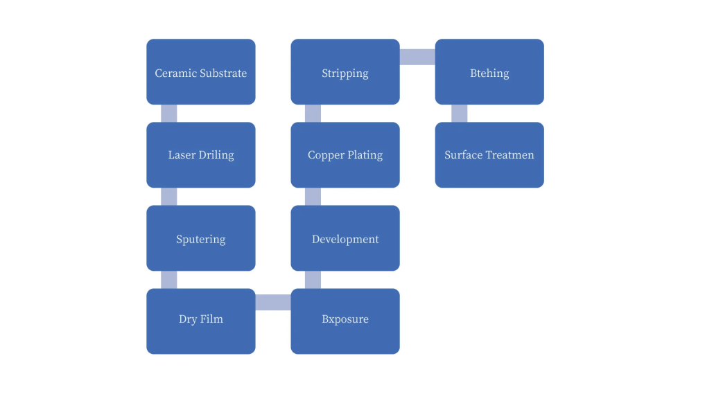
Manufacturing Process
The thin film ceramic PCB manufacturing process involves several key steps, ensuring precision and quality throughout. Below is a detailed explanation of these steps:
- Substrate Preparation: The process begins with selecting and preparing a suitable ceramic substrate, typically alumina, which is cleaned to remove any contaminants that could affect adhesion and performance.
- Thin Film Deposition: A thin film of metal, usually gold, silver, or copper, is deposited onto the ceramic substrate using techniques such as sputtering, evaporation, or chemical vapor deposition (CVD). This layer serves as the conductive path for the circuit.
- Photoresist Application: A photoresist material is applied to the metal layer, creating a mask that will define the circuit pattern. This is typically done using spin coating to achieve a uniform layer.
- Exposure and Development: The coated substrate is exposed to UV light through a photomask that contains the desired circuit pattern. The exposed areas of the photoresist are then developed, removing the unexposed regions and revealing the underlying metal.
- Etching: An etching process is employed to remove the unwanted metal from the exposed areas, leaving behind the desired circuit pattern on the substrate. This step is critical for achieving the fine features characteristic of thin film circuits.
- Photoresist Removal: After etching, the remaining photoresist is stripped away, leaving a clean, patterned metal layer on the ceramic substrate.
- Via Formation (if needed): If vertical connections between layers are required, vias can be created using laser drilling or etching techniques, allowing for multi-layer designs.
- Final Sintering: The ceramic substrate may undergo a final sintering process to enhance mechanical strength and ensure good bonding of the metal to the substrate.
- Testing and Quality Control: Each substrate is rigorously tested for electrical performance, defects, and adherence to specifications before being approved for use.
Applicable Fields
Thin Film Ceramic PCBs find applications across various high-performance sectors, including:
| Application | Description |
| Telecommunications | Used in RF components, antennas, and circuit boards for mobile and satellite communications, where signal integrity is vital. |
| Aerospace and Defense | Ideal for critical applications requiring high reliability and performance, such as radar and navigation systems. |
| Medical Devices | Employed in precision instruments and medical devices that require compact designs and high performance. |
| Consumer Electronics | Suitable for high-end consumer products like smartphones and tablets, where space is limited and performance is crucial. |
| Automotive Electronics | Used in automotive applications for control systems and sensors, benefiting from thin film technology’s reliability and performance. |
Direct Plated Copper (DPC)
Direct Plated Copper (DPC) is a modern method of depositing copper directly onto ceramic substrates, providing a flexible and efficient solution for creating high-quality ceramic PCBs. This technique is particularly advantageous for applications requiring intricate circuit designs and reliable performance.
Pros and Cons
| Pros | Cons |
| No Limitations on Ceramic Type and Thickness: DPC can be applied to various types of ceramic substrates, including different thicknesses, making it versatile for different applications. | Expensive Manufacturing Equipment: The DPC process requires advanced and specialized equipment, leading to higher initial investment costs. |
| Fine Circuits: This method allows for the creation of fine, detailed circuit patterns, essential for high-density applications and complex designs. | Process Complexity: The DPC process can be more complex than traditional methods, requiring careful control of parameters to achieve optimal results. |
| Lower Manufacturing Temperature: DPC operates at lower temperatures compared to some traditional ceramic processing methods, reducing thermal stress and the risk of damaging sensitive components. | Material Compatibility Issues: While DPC is versatile, certain materials may require specific treatment to ensure proper adhesion and performance. |
| Excellent Electrical Conductivity: The direct plating process results in a strong bond between the copper and ceramic, enhancing the electrical performance of the PCB. | Limited to Specific Applications: While DPC is effective for many applications, it may not be suitable for all types of ceramic PCBs, particularly those requiring very high precision. |
Manufacturing Process
The Direct Plated Copper manufacturing process involves several critical steps, ensuring high-quality copper deposition directly onto the ceramic substrate. Below is a detailed explanation of these steps:
- Substrate Preparation: The ceramic substrate is first cleaned and prepared to ensure a smooth surface for copper adhesion. This often includes washing to remove any contaminants and drying.
- Surface Activation: To promote adhesion, the surface of the ceramic substrate is activated, typically through a chemical treatment that modifies the surface properties. This step enhances the bonding of the copper layer.
- Copper Plating:
- Electroless Plating: A thin layer of copper is deposited onto the substrate using an electroless plating process. This involves immersing the substrate in a solution containing copper ions, which react with the substrate surface, creating a uniform copper layer without the need for an external electrical source.
- Electrolytic Plating (if necessary): Following the electroless plating, an electrolytic plating process may be used to build up the copper layer to the desired thickness. This step involves submerging the substrate in an electrolyte solution and applying an electric current, causing additional copper to deposit on the existing layer.
- Circuit Pattern Definition: After the copper layer is deposited, a photoresist material is applied to define the circuit pattern. The process includes exposure to UV light through a photomask, followed by development to remove unexposed areas, revealing the copper underneath.
- Etching: The exposed copper is then etched away using a suitable etching solution, leaving behind the desired circuit pattern on the substrate.
- Photoresist Removal: The remaining photoresist is stripped away, resulting in a clean and precise copper circuit on the ceramic substrate.
- Final Treatment: The completed PCB may undergo additional treatments, such as surface finishing to enhance solderability and protect against oxidation.
Applications in Ceramic PCB Manufacturing
Direct Plated Copper is used in a variety of applications, including:
| Application | Description |
| RF and Microwave Devices | DPC is ideal for RF components, where low-loss and high-frequency performance are crucial. |
| Power Electronics | Utilized in power management circuits, benefiting from the excellent thermal and electrical conductivity of DPC. |
| Automotive Electronics | Employed in automotive applications where reliability and performance are paramount, especially in harsh environments. |
| Medical Devices | Used in critical medical devices requiring high precision and performance, such as imaging and diagnostic equipment. |
| Consumer Electronics | Suitable for high-end consumer products, including smartphones and tablets, where miniaturization and performance are essential. |
Active Metal Brazing (AMB)
Active Metal Brazing (AMB) is a sophisticated method used to join ceramic substrates to metal components through a brazing process that utilizes an active filler material. This technique is particularly advantageous in applications requiring strong and durable bonds, making it a popular choice in industries such as aerospace and automotive.
Pros and Cons
| Pros | Cons |
| Strong Bonding: AMB produces robust joints that can withstand high mechanical and thermal stresses, ensuring long-term reliability in demanding environments. | Expensive Manufacturing Equipment: The equipment required for AMB processes can be costly, leading to higher initial investments for manufacturers. |
| Good Hot and Cold Cycle Characteristics: The joints created through AMB maintain their integrity under thermal cycling, making them suitable for applications that experience temperature fluctuations. | Limited to Two-Dimensional Circuits: AMB is not capable of producing three-dimensional circuits, which can limit its application in more complex designs. |
| High Temperature Resistance: AMB joints can withstand elevated temperatures, making them suitable for applications in harsh environments where thermal stability is essential. | Process Complexity: The AMB process can be more intricate than traditional joining methods, requiring careful control of parameters to achieve optimal bonding. |
| Excellent Chemical Resistance: AMB joints exhibit good resistance to chemical exposure, enhancing their suitability for use in corrosive environments. | Material Limitations: Not all ceramic and metal combinations may be compatible with the AMB process, potentially restricting material choices. |
Manufacturing Process
The Active Metal Brazing manufacturing process consists of several critical steps designed to create strong, reliable joints between ceramic and metal components. Below is a detailed explanation of these steps:
- Preparation of Surfaces: Both the ceramic substrate and the metal components are meticulously cleaned to remove any contaminants that could affect adhesion. Surface roughening may also be performed to enhance mechanical bonding.
- Application of Active Filler Material: A specially formulated active filler material, often containing elements like titanium or zirconium, is applied to the surfaces to be joined. This filler material plays a crucial role in facilitating bonding during the brazing process.
- Assembly: The ceramic and metal components are assembled together with the active filler in place. Care must be taken to ensure proper alignment, as this will affect the performance of the joint.
- Brazing Process:
- Heating: The assembled components are then subjected to controlled heating in a vacuum or inert atmosphere. This step is critical to prevent oxidation and to ensure a clean bonding environment.
- Melting of Filler Material: As the temperature increases, the active filler material melts, flowing into the joint interface. The melting point of the filler is typically lower than that of the ceramic and metal components.
- Diffusion Bonding: The active elements in the filler material react with the surfaces of the ceramic and metal, promoting diffusion and resulting in a strong metallurgical bond once cooled.
- Cooling: After sufficient bonding time at elevated temperatures, the assembly is allowed to cool gradually. This cooling process is essential to avoid thermal shock, which could damage the materials.
- Post-Bonding Treatment: The bonded assembly may undergo additional treatments, such as machining or surface finishing, to achieve the desired specifications and performance characteristics.
Applications in Aerospace and Automotive Fields
Active Metal Brazing is widely utilized in various applications across the aerospace and automotive industries due to its ability to create strong, reliable joints. Some specific applications include:
| Application | Description |
| Aerospace Components | AMB is used to join ceramic components in turbine engines, where high-temperature resistance and mechanical strength are crucial. |
| Heat Exchangers | The method is employed in the manufacturing of heat exchangers, where durability and thermal performance are essential. |
| Sensor Assemblies | AMB is utilized for joining ceramic sensors in automotive systems, providing reliable performance under varying conditions. |
| Combustion Chambers | In aerospace applications, AMB is used to create robust joints in combustion chambers, ensuring they can withstand extreme temperatures and pressures. |
| Fuel Cell Systems | AMB is suitable for fuel cell applications, where strong and thermally stable joints are necessary for efficient operation. |
FAQs About ceramic substrate manufacturing process
Ceramic substrates are typically made through a series of steps that involve selecting raw materials, shaping, drying, and firing the products. The process generally includes:
Raw Material Selection: Common materials include alumina, zirconia, or other ceramic powders.
Mixing: The raw materials are mixed with additives to enhance properties like plasticity and strength.
Shaping: The mixed materials are shaped using methods such as pressing, extrusion, or casting to form the desired substrate.
Drying: The shaped substrates are dried to remove moisture and prepare for firing.
Firing: The dried substrates are fired in a kiln at high temperatures, typically between 800°C to 1,600°C, to achieve the desired mechanical and electrical properties.
The manufacturing process for ceramic products generally follows these steps:
Raw Material Preparation: Selection and grinding of raw materials, such as clay, feldspar, and silica.
Forming: Techniques such as pressing, extrusion, or slip casting are used to shape the ceramic into desired forms.
Drying: The shaped products are dried to remove excess moisture and prevent cracking during firing.
Firing: Dried ceramics are fired in a kiln at high temperatures to achieve hardness and durability. This process can also include glaze application for decorative products.
Finishing: After firing, products may undergo finishing processes, such as polishing, cutting, or coating, to enhance their appearance or performance.
The composition of ceramic substrates typically includes:
Alumina (Al₂O₃): Often the primary material, providing excellent thermal stability and electrical insulation.
Silica (SiO₂): Used to enhance the substrate’s mechanical strength and thermal properties.
Zirconia (ZrO₂): Occasionally included for improved toughness and thermal stability.
Additives: Various additives may be used to modify properties, including fluxes for melting point adjustment and binders to improve workability.
The manufacturing process for ceramic bricks typically involves the following steps:
Raw Material Selection: Clay, shale, or other natural materials are selected for their properties.
Preparation: The raw materials are crushed and mixed, often with water, to create a homogeneous clay mixture.
Forming: The mixture is shaped into bricks using methods such as extrusion or molding.
Drying: The formed bricks are dried to reduce moisture content and prevent cracking during firing.
Firing: The dried bricks are fired in a kiln at high temperatures (around 900°C to 1,200°C) to achieve hardness and durability.
Cooling and Quality Control: After firing, bricks are cooled gradually, and quality checks are conducted to ensure they meet specifications.

