
Shinko Substrate: Ensuring Reliable Chip Support
Shinko Electric Industries Co., Ltd., commonly known as Shinko, is a leading company in the semiconductor industry, renowned for its innovative technologies and high-quality products. Established in 1946, Shinko has consistently contributed to the advancement of semiconductor packaging and interconnect solutions. The company specializes in manufacturing substrates, leadframes, and various other components essential for semiconductor devices. Shinko’s products play a crucial role in ensuring the performance and reliability of electronic devices, making them a key player in the global semiconductor supply chain.
The purpose of this blog post is to provide a comprehensive introduction to Shinko substrates and related technologies and products. We will explore the core concepts of Shinko substrates, their applications, and the differences between substrates and leadframes. Additionally, we will delve into advanced products such as coreless substrates and integrated thermal management solutions, highlighting Shinko’s contributions to the semiconductor industry’s evolution.
Overview of Shinko Industries
Company History and Development
Shinko Electric Industries Co., Ltd., established in 1946, began its journey as a manufacturer of electrical components. Over the decades, Shinko has evolved into a pivotal player in the semiconductor industry, driven by a commitment to innovation and quality. Initially focused on basic electrical parts, the company shifted its focus towards semiconductor packaging solutions in response to the burgeoning demand for advanced electronic devices. By the 1970s, Shinko had made significant strides in developing cutting-edge semiconductor components, cementing its reputation as a technological leader.
Throughout its history, Shinko has continually expanded its technological capabilities and production capacity. The company has invested heavily in research and development, enabling it to introduce pioneering products such as multilayer substrates and high-performance leadframes. Today, Shinko operates multiple state-of-the-art manufacturing facilities worldwide, ensuring a robust supply chain and meeting the global demand for high-quality semiconductor components.
Key Business Areas and Product Lines
Shinko’s core business revolves around the development and production of semiconductor packaging materials and components. The company’s product portfolio is diverse, catering to various segments of the semiconductor industry. Key business areas and product lines include:
- Substrates: Shinko specializes in manufacturing advanced substrates, including organic substrates and coreless substrates, which are integral to semiconductor packaging. These substrates offer high-density interconnections and superior thermal management, essential for modern electronic devices.
- Leadframes: Shinko produces a wide range of leadframes used in semiconductor devices. These leadframes are crucial for providing electrical connections and mechanical support to semiconductor chips, ensuring their functionality and durability.
- Multi-Chip Embedded Package (MCEP): This innovative product line involves embedding multiple semiconductor chips within a single package, enhancing performance and reducing space requirements. MCEP solutions are vital for high-performance computing and telecommunications applications.
- Integrated Thermal Management Solutions (IThop): Shinko’s IThop solutions address the critical need for effective thermal management in semiconductor devices. These solutions help dissipate heat efficiently, ensuring optimal performance and longevity of electronic components.
- Electro-Mechanical Components: Beyond semiconductor packaging, Shinko also manufactures a variety of electro-mechanical components, further broadening its product offerings.
Shinko’s unwavering focus on quality and innovation has solidified its position as a trusted supplier in the semiconductor industry. The company’s products are widely used in various applications, from consumer electronics to industrial machinery, underscoring its versatility and technological prowess. As the semiconductor industry continues to evolve, Shinko remains at the forefront, driving advancements and setting new standards in semiconductor packaging and interconnect solutions.
What is Shinko Substrate?
Definition and Basic Concepts
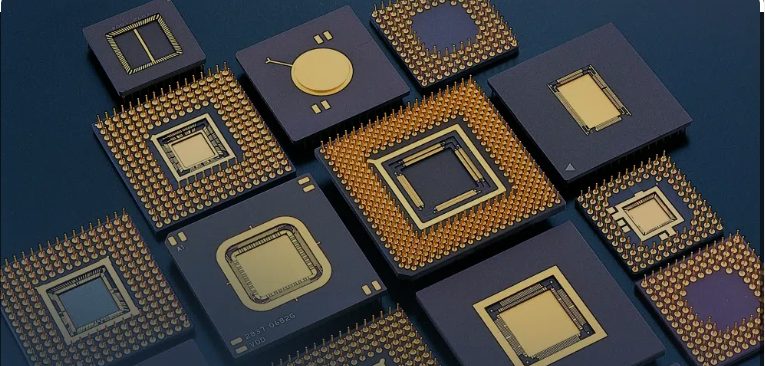
A Shinko substrate is a key component in semiconductor packaging, serving as the foundation upon which semiconductor devices are built and interconnected. Substrates provide the necessary physical and electrical support for semiconductor chips, enabling them to function correctly within electronic devices. Shinko substrates are typically made from high-performance materials such as organic compounds or ceramics, designed to offer excellent thermal and electrical properties.
The primary function of a substrate is to facilitate the connection between the semiconductor chip and the external circuitry. This involves creating a stable base for the chip, providing electrical pathways through conductive traces, and managing thermal dissipation to ensure the chip operates within safe temperature ranges. Shinko’s substrates are known for their high-density interconnection capabilities, which allow for more complex and compact semiconductor designs.
Applications in Semiconductor Manufacturing
Shinko substrates play a crucial role in various stages of semiconductor manufacturing and are essential for the performance and reliability of modern electronic devices. Key applications include:
- Integrated Circuit (IC) Packaging:
- Shinko substrates are widely used in the packaging of integrated circuits, which are the building blocks of most electronic devices. These substrates provide the platform for mounting ICs, connecting them electrically to other components, and protecting them from physical damage and environmental factors.
- System in Package (SiP):
- In SiP technology, multiple semiconductor chips and passive components are integrated into a single package. Shinko substrates enable this integration by offering multi-layer interconnections and efficient thermal management, resulting in compact and high-performance packages used in smartphones, tablets, and other portable devices.
- Flip-Chip Technology:
- Shinko substrates are essential for flip-chip packaging, where the semiconductor chip is flipped and mounted directly onto the substrate. This technique allows for shorter interconnections, reduced signal latency, and improved electrical performance, making it ideal for high-speed computing and communication applications.
- Advanced Driver Assistance Systems (ADAS):
- In automotive electronics, Shinko substrates are used in ADAS to support sensors, cameras, and radar systems. These substrates ensure reliable performance and durability under harsh operating conditions, contributing to the safety and functionality of modern vehicles.
- High-Performance Computing (HPC):
- For HPC applications, such as data centers and supercomputers, Shinko substrates provide the necessary high-density interconnections and efficient thermal management required to support powerful processors and memory modules.
- Consumer Electronics:
- Shinko substrates are integral to the manufacturing of various consumer electronics, including laptops, gaming consoles, and wearable devices. They enable the miniaturization and enhanced functionality of these devices by supporting advanced packaging technologies.
Shinko substrates are critical in the semiconductor industry’s drive towards miniaturization, higher performance, and greater energy efficiency. Their advanced materials and manufacturing techniques ensure that electronic devices can meet the ever-increasing demands of modern applications, from high-speed data processing to complex, multifunctional systems. As the semiconductor landscape continues to evolve, Shinko substrates will remain at the forefront, enabling the next generation of electronic innovations.
Difference Between Substrate and Leadframe
Functions and Characteristics of a Substrate
A substrate in semiconductor packaging serves as the foundational layer that supports and interconnects semiconductor chips. The key functions and characteristics of a substrate include:
- Electrical Interconnection: Substrates provide the electrical pathways that connect the semiconductor chip to the external circuitry. These pathways are formed by conductive traces embedded within the substrate material.
- Thermal Management: Substrates are designed to dissipate heat generated by the semiconductor chip during operation. Effective thermal management is crucial to maintain the chip’s performance and reliability.
- Mechanical Support: Substrates offer a stable platform for mounting semiconductor chips, protecting them from physical stress and damage.
- Material Composition: Substrates are typically made from high-performance materials such as organic compounds (e.g., BT resin) or ceramics, which offer excellent electrical and thermal properties.
- Multi-Layer Structures: Many substrates are multi-layered, allowing for high-density interconnections and more complex circuit designs.
Functions and Characteristics of a Leadframe
A leadframe is another essential component in semiconductor packaging, primarily used in traditional and cost-effective packaging methods. The key functions and characteristics of a leadframe include:
- Electrical Connection: Leadframes provide a framework of metal leads that connect the semiconductor chip to external circuitry. These leads extend from the chip to the outside of the package, facilitating electrical connectivity.
- Mechanical Support: Leadframes offer structural support to the semiconductor chip, ensuring it remains securely in place within the package.
- Heat Dissipation: Some leadframes incorporate heat sinks or thermal pads to help dissipate heat away from the semiconductor chip, though their thermal management capabilities are generally less advanced than those of substrates.
- Material Composition: Leadframes are typically made from metal, such as copper or a copper alloy, which provides good electrical conductivity and mechanical strength.
- Single-Layer Structure: Unlike substrates, leadframes are usually single-layer structures, which makes them less suitable for high-density interconnection but more cost-effective for simpler applications.
Key Differences in Applications and Manufacturing Processes
The differences between substrates and leadframes are evident in their applications and manufacturing processes:
- Applications:
- Substrates: Substrates are commonly used in advanced semiconductor packaging technologies, such as Ball Grid Array (BGA), Chip Scale Package (CSP), and Flip-Chip. These applications require high-density interconnections, excellent thermal management, and the ability to support complex circuit designs. Substrates are preferred in high-performance computing, telecommunications, and consumer electronics where miniaturization and high functionality are crucial.
- Leadframes: Leadframes are typically used in more traditional packaging methods like Dual In-Line Package (DIP) and Quad Flat Package (QFP). These methods are suitable for less complex and cost-sensitive applications, such as standard consumer electronics, automotive components, and some industrial devices.
- Manufacturing Processes:
- Substrates: The manufacturing of substrates involves advanced processes such as photolithography, electroplating, and lamination. Multi-layer substrates require precise alignment and bonding of several thin layers, each with its own pattern of conductive traces. This complexity allows for higher performance but also results in higher production costs.
- Leadframes: Leadframe manufacturing is more straightforward, involving stamping or etching metal sheets to create the desired pattern of leads. The process is highly efficient and cost-effective, making leadframes an economical choice for many applications. However, this simplicity limits the complexity and density of interconnections that can be achieved.
Substrates and leadframes serve similar fundamental purposes in semiconductor packaging, but they differ significantly in their specific functions, characteristics, and suitable applications. Substrates offer advanced capabilities for high-performance and complex devices, while leadframes provide a cost-effective solution for simpler and more traditional semiconductor packages. Understanding these differences is crucial for selecting the appropriate packaging technology based on the requirements of the specific application.
What is a Coreless Substrate?
Core Features and Advantages
Coreless substrates are an advanced type of semiconductor packaging substrate that, as the name implies, lack the central core layer found in traditional substrates. This innovative design offers several key features and advantages:
- Reduced Thickness: The absence of a core layer significantly reduces the overall thickness of the substrate. This is particularly beneficial in applications where space is at a premium, such as in mobile devices and other compact electronics.
- Enhanced Flexibility: Coreless substrates are more flexible than their core-based counterparts, which can be advantageous in applications requiring bending or conformability.
- Improved Electrical Performance: By eliminating the core layer, coreless substrates reduce the length of electrical paths between the semiconductor chip and the external circuitry. This reduction minimizes signal loss and latency, resulting in improved electrical performance, especially at high frequencies.
- Superior Thermal Management: The design of coreless substrates allows for better heat dissipation. With fewer layers and better thermal conductivity pathways, heat generated by the semiconductor chip is more efficiently dispersed, enhancing the reliability and longevity of the device.
- Higher Density Interconnections: Coreless substrates support finer line widths and smaller via sizes, allowing for higher density interconnections. This capability is crucial for advanced semiconductor packages that require more I/O connections and increased functionality within a smaller footprint.
- Reduced Warpage: The absence of a core layer reduces the tendency of the substrate to warp during thermal cycling, which is a common issue in traditional substrates. This stability enhances the overall reliability of the semiconductor package.
Applications in Semiconductor Packaging
Coreless substrates are particularly well-suited for advanced semiconductor packaging applications that demand high performance, miniaturization, and reliability. Key applications include:
- Mobile Devices:
- Smartphones and tablets benefit significantly from coreless substrates due to their need for compact, lightweight, and high-performance components. The reduced thickness and enhanced electrical performance of coreless substrates make them ideal for these applications.
- High-Performance Computing (HPC):
- In HPC applications, such as data centers and supercomputers, coreless substrates enable the integration of powerful processors and memory modules. The high-density interconnections and superior thermal management provided by coreless substrates are essential for supporting the intensive computational demands of HPC environments.
- Wearable Electronics:
- Wearable devices, including smartwatches and fitness trackers, require substrates that are not only thin and lightweight but also flexible. Coreless substrates meet these requirements, allowing for the development of comfortable and durable wearable technology.
- Advanced Driver Assistance Systems (ADAS):
- The automotive industry relies on coreless substrates for ADAS, which includes radar, lidar, and camera systems. These applications require reliable and high-performance packaging solutions that can withstand harsh operating conditions, making coreless substrates an ideal choice.
- Internet of Things (IoT) Devices:
- IoT devices, ranging from smart home appliances to industrial sensors, benefit from the compact and efficient design of coreless substrates. These substrates enable the integration of multiple functions into small, energy-efficient packages.
- Telecommunications:
- Coreless substrates are crucial in telecommunications equipment, where they support the high-frequency operation of components such as RF modules and baseband processors. The improved electrical performance and reduced signal loss are particularly advantageous in this field.
- Consumer Electronics:
- Beyond mobile devices and wearables, coreless substrates find applications in a wide range of consumer electronics, including gaming consoles, digital cameras, and home entertainment systems. Their ability to support high-density interconnections and efficient thermal management enhances the performance and reliability of these devices.
Coreless substrates represent a significant advancement in semiconductor packaging technology. Their unique features and advantages make them indispensable in a variety of high-performance and compact applications. As the demand for more powerful, efficient, and miniaturized electronic devices continues to grow, coreless substrates are set to play a pivotal role in meeting these evolving requirements.
Key Products and Technologies of Shinko
Shinko Substrate: Technical Specifications and Advantages
Technical Specifications:
- Materials: Shinko substrates are typically made from advanced materials such as organic resins (e.g., BT resin), ceramics, and advanced polymers.
- Layer Count: They can be multi-layered, supporting high-density interconnections through multiple thin layers.
- Line Widths and Spacing: Shinko substrates offer fine line widths and spacing, often down to micrometer scales, which is essential for high-density packaging.
- Via Sizes: They feature microvias, allowing for dense and efficient electrical connections between layers.
- Thermal Conductivity: High thermal conductivity materials are used to enhance heat dissipation.
- Mechanical Properties: Designed for robustness to withstand mechanical stress and thermal cycling.
Advantages:
- High-Density Interconnections: Supports complex circuitry and high I/O counts, making them ideal for advanced electronic devices.
- Superior Thermal Management: Efficiently dissipates heat, ensuring reliable performance and longevity of semiconductor devices.
- Compact Design: Enables miniaturization, which is crucial for modern electronics such as smartphones and wearables.
- Enhanced Electrical Performance: Low signal loss and high-speed data transmission capabilities.
- Reliability: Reduced warpage and improved mechanical stability contribute to the overall reliability of the package.
Shinko Leadframe: Technical Specifications and Application Areas
Technical Specifications:
- Materials: Typically made from metals like copper, copper alloys, and occasionally silver or gold plating for enhanced conductivity.
- Dimensions: Can be tailored to specific device requirements, with precise lead dimensions and pitches.
- Plating: Surface plating options to improve solderability and corrosion resistance.
- Thermal Pads: Some leadframes include integrated thermal pads for better heat dissipation.
Application Areas:
- Standard IC Packaging: Widely used in traditional IC packages such as Dual In-Line Packages (DIP), Quad Flat Packages (QFP), and Small Outline Packages (SOP).
- Power Devices: Ideal for power electronics where efficient heat dissipation and robust mechanical support are required.
- Automotive Electronics: Used in various automotive applications, offering reliability under harsh conditions.
- Consumer Electronics: Common in household electronic devices due to their cost-effectiveness and reliability.
Shinko MCEP (Multi-Chip Embedded Package): Overview and Applications
Overview: Shinko’s Multi-Chip Embedded Package (MCEP) technology involves embedding multiple semiconductor chips within a single package. This advanced packaging solution integrates different types of chips and passive components into one compact module, enhancing performance and functionality.
Applications:
- Mobile Devices: Enables the integration of processors, memory, and other components into a single, compact package, reducing space and improving performance.
- High-Performance Computing: Used in servers and data centers where multiple chips need to work together efficiently in close proximity.
- Telecommunications: Enhances the performance of communication devices by integrating RF, baseband, and other components into one package.
- Automotive Systems: Applied in advanced automotive systems where space and performance are critical, such as in ADAS and infotainment systems.
Shinko IThop (Integrated Thermal Management Solutions): Overview and Applications
Overview: Shinko’s Integrated Thermal Management Solutions (IThop) address the critical need for efficient heat dissipation in high-performance semiconductor devices. These solutions integrate thermal management features directly into the packaging design, ensuring effective heat removal.
Applications:
- High-Power Devices: Essential for power electronics and devices that generate significant heat, such as power amplifiers and LED drivers.
- High-Performance Computing: Crucial in data centers and supercomputers where efficient cooling is necessary to maintain performance and prevent overheating.
- Automotive Electronics: Used in automotive systems to manage the heat generated by high-power components, ensuring reliability and safety.
- Consumer Electronics: Helps maintain optimal performance and extend the lifespan of high-performance consumer devices like gaming consoles and high-end laptops.
Shinko offers a diverse range of advanced products and technologies that address various needs in semiconductor packaging. From high-density interconnection substrates to robust and efficient leadframes, multi-chip embedded packages, and integrated thermal management solutions, Shinko’s offerings are pivotal in advancing the performance and reliability of modern electronic devices. As technology continues to evolve, Shinko remains at the forefront, driving innovation and setting new standards in semiconductor packaging.
Market Prospects and Development Trends
Future Trends in the Semiconductor Industry
The semiconductor industry is on the cusp of several transformative trends that are expected to shape its future trajectory. Key trends include:
- Miniaturization and Increased Complexity: As electronic devices become more powerful and compact, the demand for smaller, more complex semiconductor packages continues to rise. This drives advancements in packaging technologies such as system-in-package (SiP) and multi-chip modules (MCM).
- 5G and Beyond: The rollout of 5G networks and the development of 6G are pushing the limits of semiconductor technology. These technologies require high-frequency, high-performance components, leading to greater demand for advanced substrates and packaging solutions.
- Artificial Intelligence (AI) and Machine Learning (ML): AI and ML applications necessitate high-performance computing capabilities. This trend drives the need for substrates and packages that can support high-speed data processing and efficient thermal management.
- Internet of Things (IoT): The proliferation of IoT devices, from smart home gadgets to industrial sensors, demands innovative packaging solutions that are both compact and energy-efficient.
- Automotive Electronics: The automotive industry is rapidly adopting advanced electronics for autonomous driving, safety systems, and infotainment. This requires robust, reliable, and high-performance semiconductor packages.
- Sustainability and Energy Efficiency: There is an increasing focus on sustainability within the semiconductor industry. This includes the development of energy-efficient components and environmentally friendly manufacturing processes.
Shinko’s Competitive Advantages and Market Outlook
Shinko Electric Industries is well-positioned to capitalize on these emerging trends due to several competitive advantages:
Competitive Advantages:
- Technological Leadership: Shinko is at the forefront of semiconductor packaging technology, consistently investing in research and development to innovate and improve its product offerings.
- Advanced Manufacturing Capabilities: With state-of-the-art manufacturing facilities, Shinko can produce high-quality substrates and leadframes with exceptional precision and efficiency.
- Diverse Product Portfolio: Shinko offers a wide range of products, including advanced substrates, leadframes, multi-chip embedded packages (MCEP), and integrated thermal management solutions (IThop). This diversity allows Shinko to meet the varied needs of its customers across different applications and industries.
- Customization and Flexibility: Shinko’s ability to provide customized solutions tailored to specific customer requirements enhances its competitiveness, particularly in high-performance and specialized applications.
- Quality and Reliability: Shinko’s commitment to quality ensures that its products meet the highest standards, providing reliability and performance that customers can trust.
Market Outlook:
- Growth in Mobile and Consumer Electronics: With the continuous evolution of smartphones, tablets, and wearable devices, Shinko’s advanced substrates and multi-chip packages will see increasing demand.
- Expansion in High-Performance Computing: As data centers and supercomputers evolve, the need for efficient and high-density packaging solutions will grow, benefiting Shinko’s advanced product lines.
- Automotive Industry Opportunities: The rapid advancement in automotive electronics, including ADAS and autonomous driving technologies, presents significant growth opportunities for Shinko’s robust and reliable packaging solutions.
- IoT Proliferation: The expanding IoT ecosystem will drive demand for Shinko’s compact and energy-efficient packaging solutions, particularly in smart home, industrial, and healthcare applications.
- 5G and Telecommunications: The ongoing deployment of 5G and future 6G networks will require advanced substrates and packaging solutions that support high-frequency operation and enhanced performance, areas where Shinko excels.
The semiconductor industry is poised for significant growth and transformation, driven by trends such as miniaturization, 5G, AI, IoT, and advancements in automotive electronics. Shinko, with its technological leadership, advanced manufacturing capabilities, diverse product portfolio, and commitment to quality, is well-positioned to capitalize on these trends. The company’s competitive advantages and strategic focus on innovation and customer-centric solutions will enable it to maintain and strengthen its market position, ensuring robust growth in the years to come.
How to Purchase Shinko Products
Purchase Channels and Main Suppliers
Purchase Channels:
- Direct Sales: Shinko Electric Industries offers direct sales channels through their official website and sales representatives. This approach ensures that customers receive authentic products and can benefit from personalized service, including technical support and customization options.
- Authorized Distributors: Shinko collaborates with a network of authorized distributors worldwide. These distributors are vetted and approved by Shinko to ensure they meet the company’s standards for quality and service. Purchasing from authorized distributors guarantees access to genuine Shinko products and often includes additional support services.
- Online Platforms: Some authorized distributors and Shinko itself may offer products through major online B2B platforms such as Digi-Key, Mouser Electronics, and Arrow Electronics. These platforms provide a convenient way to browse and purchase Shinko products, especially for smaller orders or prototyping needs.
- Trade Shows and Expos: Shinko frequently participates in industry trade shows and expos. These events are excellent opportunities to meet with Shinko representatives, see product demonstrations, and place orders for new and existing products.
Main Suppliers:
- Digi-Key Electronics: A major distributor of electronic components, offering a wide range of Shinko products with detailed product information and fast shipping options.
- Mouser Electronics: Another key distributor, providing comprehensive listings of Shinko products, including datasheets and customer reviews.
- Arrow Electronics: Known for its extensive inventory and support services, Arrow Electronics is a reliable source for Shinko components.
- Avnet: Avnet offers a robust selection of Shinko products, coupled with strong technical support and supply chain services.
Tips for Selecting Shinko Products
Understand Your Requirements:
- Application Needs: Clearly define the application for which you need Shinko products. Different applications may require specific types of substrates, leadframes, or thermal management solutions. For instance, high-frequency applications might need substrates with superior electrical performance, while automotive applications might prioritize robustness and thermal management.
- Performance Specifications: Identify the critical performance specifications for your project, such as thermal conductivity, electrical properties, size constraints, and mechanical stability. Comparing these requirements with Shinko’s product specifications will help you select the most suitable product.
Consult Technical Documentation:
- Datasheets and Application Notes: Thoroughly review the datasheets and application notes available for Shinko products. These documents provide detailed technical specifications, recommended usage guidelines, and performance characteristics.
- Case Studies and White Papers: Look for case studies and white papers that illustrate how Shinko products have been used in similar applications. These resources can offer insights into practical considerations and performance outcomes.
Leverage Support Services:
- Technical Support: Utilize the technical support services offered by Shinko and its distributors. Their experts can provide valuable advice on product selection, customization options, and integration into your existing systems.
- Design Assistance: Many distributors offer design assistance services, helping you optimize your design for the chosen Shinko products. This can include layout recommendations, thermal analysis, and simulation support.
Evaluate Supplier Credentials:
- Authorized Distributors: Ensure that you purchase from authorized distributors to guarantee the authenticity and quality of Shinko products. Authorized distributors also provide warranty and after-sales support.
- Customer Reviews and Feedback: Check customer reviews and feedback on the distributor’s website or third-party platforms. This can give you an idea of the distributor’s reliability and service quality.
Consider Total Cost of Ownership:
- Price vs. Performance: While it’s essential to consider the cost of Shinko products, it’s equally important to evaluate their performance and reliability. High-quality components can reduce long-term costs by minimizing failures and maintenance needs.
- Supply Chain Stability: Assess the distributor’s supply chain stability and lead times. Reliable supply chains ensure that you receive your products on time, which is crucial for maintaining production schedules.
Sample and Prototype Testing:
- Request Samples: Before making a large purchase, request samples of Shinko products to test in your specific application. This helps verify performance and compatibility.
- Prototype Testing: Conduct thorough testing with prototypes to ensure the selected products meet all performance and reliability criteria. This step can prevent costly redesigns and production delays.
By following these guidelines, you can effectively navigate the purchasing process for Shinko products, ensuring that you select the best components for your specific needs and applications.
FAQs About shinko substrate
Difference between Substrate and Leadframe:
Substrate: A substrate is a foundational layer in semiconductor packaging that provides structural support and electrical interconnections for semiconductor chips. It is typically made from materials like organic resins or ceramics and features multiple layers with fine conductive traces. Substrates are crucial for high-density packaging and advanced semiconductor devices.
Leadframe: A leadframe is a metal structure used in semiconductor packaging to provide electrical connections between the semiconductor chip and external circuitry. Leadframes are typically made from metals like copper and feature a grid of leads that extend from the chip to the package’s exterior. They offer mechanical support and facilitate heat dissipation but are less suitable for high-density interconnections compared to substrates.
A coreless substrate is a type of semiconductor packaging substrate that lacks a central core layer found in traditional substrates. Instead of a core, coreless substrates feature multiple layers of substrate material, often made from advanced organic resins or ceramics. Coreless substrates offer advantages such as reduced thickness, enhanced flexibility, improved electrical performance, superior thermal management, and higher density interconnections. They are commonly used in applications where space, performance, and reliability are critical.
Shinko Electric Industries Co., Ltd., commonly known as Shinko, was established in 1946 in Japan. Initially, the company focused on manufacturing electrical components. Over the years, Shinko expanded its operations and shifted its focus to semiconductor packaging solutions in response to the growing demand for advanced electronic devices.
Throughout its history, Shinko has remained committed to innovation and quality, investing in research and development to develop cutting-edge technologies and products. The company has continuously expanded its manufacturing capabilities and global presence, establishing itself as a leading supplier in the semiconductor industry.
Today, Shinko offers a diverse range of products, including substrates, leadframes, multi-chip embedded packages (MCEP), and integrated thermal management solutions. With its technological expertise, advanced manufacturing facilities, and commitment to customer satisfaction, Shinko continues to drive advancements in semiconductor packaging and interconnect solutions.

