
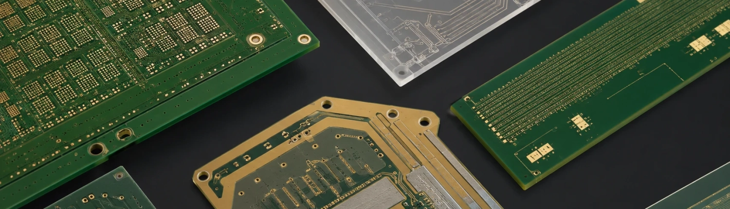
ALCANTA provides a wide range of substrate solutions for semiconductor packaging, fine-line interconnections,glass-based electronics,narow-format structures and mult-material aplications.
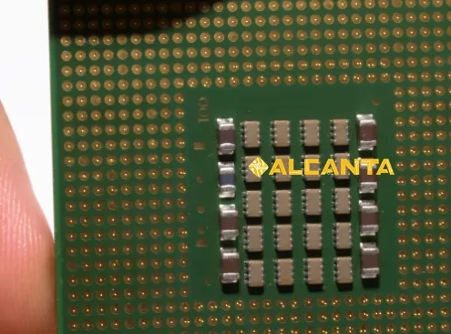
BT Substrates
BT substrates provide stable electrical performance, heat resistance and dimensional reliability for semiconductor packaging, LED modules and compact electronic devices.
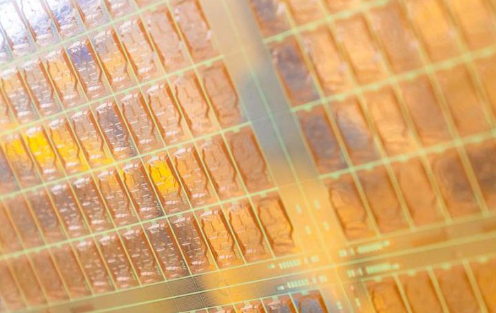
Glass Substrates
Glass substrates provide excellent flatness, dimensional stability and insulation for advanced packaging, sensors and optoelectronic applications.
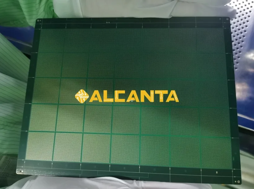
ABF Substrates
ABF build-up substrates support fine-line routing, microvias and high-density multilayer interconnections for advanced semiconductor packaging.
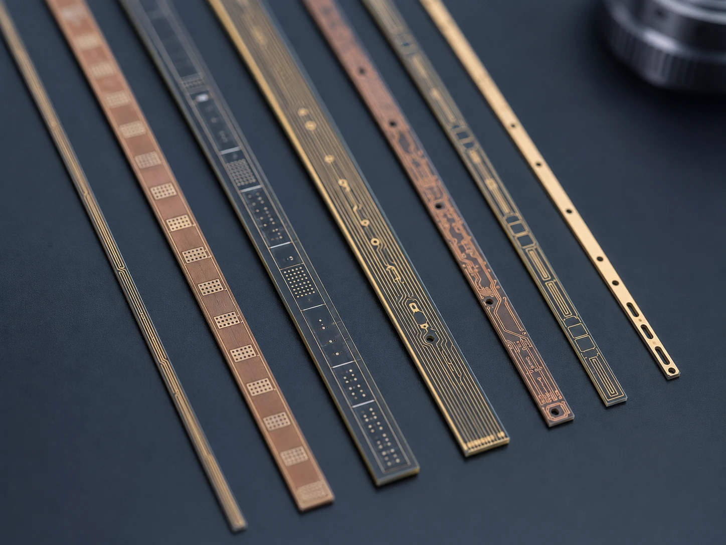
Narrow-Format Substrates
Narrow-format substrates are designed for space-constrained products, elongated structures and compact electronic devices.
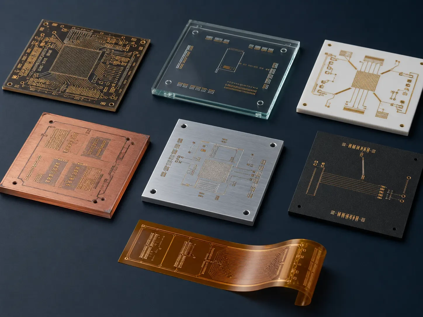
Multi-Material Substrates
Hybrid substrate structures combine organic, glass, ceramic or metal-based materials to meet electrical, thermal and mechanical requirements.
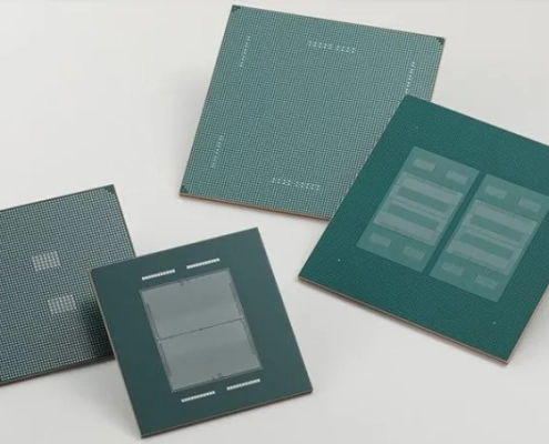
Custom Substrate Solutions
Application-specific substrates are developed around customer materials, dimensions, circuit structures and manufacturing requirements.
Our Core Manufacturing Capabilities
Fine-Line Circuits
Fine line and space capability down to 9 μm / 9 μm, depending on material and structure.
Microvias
Minimum via diameter down to 55 μm, depending on material, thickness and via structure.
Multiple Materials
Support for organic, glass, ceramic, metal-based, high-frequency and custom materials.
Custom Dimensions
Width, length, thickness and outline customized according to project requirements.
Final capabilities depend on material type, substrate structure, dimensions and design requirements.


