
Circuit Substrate: Key Element in Electronics
A circuit substrate, commonly referred to as the base material of a printed circuit board (PCB), is a foundational component in electronic circuits. It provides the physical support for electronic components and the necessary pathways for electrical connections. Substrates are typically made from insulating materials, such as fiberglass epoxy (FR4), ceramics, or polyimides, which ensure electrical isolation between conductive paths.
The importance of a circuit substrate in electronic circuits cannot be overstated. It not only supports and connects the electronic components but also influences the circuit’s overall performance, reliability, and thermal management. The choice of substrate material impacts the PCB’s mechanical strength, thermal conductivity, and electrical properties, all of which are crucial for the functionality and longevity of electronic devices. As electronic devices become more advanced and miniaturized, the role of high-quality, efficient substrates becomes increasingly vital in achieving optimal performance and durability.
Overview of Printed Circuit Boards (PCBs) with Circuit Substrate
Definition and Function
A printed circuit board (PCB) is a flat board that houses interconnected electronic components. It uses conductive tracks, pads, and other features etched from copper sheets laminated onto a non-conductive circuit substrate. The primary function of a PCB is to mechanically support and electrically connect electronic components using conductive pathways, tracks, or signal traces. These pathways are essential for directing electrical currents to different parts of the circuit, ensuring the device operates as intended.
Common Types of PCBs
PCBs come in various types, each designed to meet specific needs and applications. The type of circuit substrate used plays a crucial role in defining the characteristics and capabilities of the PCB. Here are the most common types:
Single-sided PCBs
Single-sided PCBs have a single layer of conductive material on one side of the circuit substrate. These are the simplest and most cost-effective types of PCBs, typically used in low-density designs where component placement is minimal, such as in consumer electronics and simple gadgets.
Double-sided PCBs
Double-sided PCBs feature conductive material on both sides of the circuit substrate. This allows for more complex circuits and a higher density of components. Connections between the two sides are made using vias (small holes plated with conductive material), enabling more intricate circuit designs often found in industrial controls, automotive systems, and power supplies.
Multi-layer PCBs
Multi-layer PCBs consist of multiple layers of conductive material separated by insulating layers of circuit substrate. These layers are laminated together under high pressure and temperature to form a single, compact board. Multi-layer PCBs are used in advanced, high-performance electronics like smartphones, computers, and medical devices due to their ability to support complex and high-density circuitry.
Rigid PCBs
Rigid PCBs are made from a solid, inflexible circuit substrate. They maintain their shape and integrity under mechanical stress, making them suitable for a wide range of applications, including consumer electronics, automotive electronics, and industrial machinery. The rigidity of these boards provides a stable platform for component mounting and interconnections.
Flexible PCBs
Flexible PCBs use a flexible circuit substrate, such as polyimide, allowing the board to bend and flex without breaking. This flexibility enables their use in applications where space is constrained and the circuit needs to conform to a specific shape, such as in wearable devices, medical equipment, and flexible displays.
Rigid-flex PCBs
Rigid-flex PCBs combine the benefits of both rigid and flexible circuit substrates. These boards have both rigid and flexible sections, allowing for complex designs that require a stable structure while providing the flexibility needed to fit into tight spaces. They are commonly used in advanced electronics like aerospace, military applications, and high-end consumer electronics.
The choice of circuit substrate and the type of PCB are critical factors that influence the performance, reliability, and application of the electronic device. Understanding the different types of PCBs and their substrates helps in designing and manufacturing efficient and robust electronic systems.
Types of Circuit Board Substrates
Circuit substrates are essential in defining the physical and electrical characteristics of a printed circuit board (PCB). Different materials are used as substrates, each offering unique properties suited for specific applications. Here is an in-depth look at the various types of circuit board substrates:
FR4 (Fiberglass Epoxy)
Properties and Uses: FR4 is the most commonly used circuit substrate material. It is made from woven fiberglass cloth with an epoxy resin binder that is flame resistant (hence the designation “FR”). This substrate offers a good balance of strength, durability, and electrical insulation. FR4 substrates are known for their excellent mechanical properties, moisture resistance, and relatively low cost.
Uses:
- Consumer electronics
- Computer hardware
- Telecommunications
- Automotive electronics
Metal Core PCB (MCPCB)
Thermal Management and Applications: Metal Core PCBs have a metal (usually aluminum or copper) as their base circuit substrate. This metal core helps in efficiently dissipating heat away from the components, which is crucial for high-power and high-temperature applications. The metal core acts as a heat sink, improving the thermal performance of the PCB.
Applications:
- LED lighting
- Power supplies
- Motor controllers
- High-current circuits
Ceramic Substrates
High-frequency Applications: Ceramic substrates, made from materials like alumina (Al2O3) or aluminum nitride (AlN), offer excellent thermal conductivity and can withstand high temperatures. They also have superior electrical insulation properties and low dielectric loss, making them ideal for high-frequency and microwave applications.
Applications:
- RF (radio frequency) modules
- Microwave circuits
- High-frequency communication devices
- Power electronics
Polyimide
Flexible Circuits: Polyimide is a polymer material used as a circuit substrate in flexible PCBs. It offers high thermal stability, excellent chemical resistance, and flexibility, making it suitable for applications where the PCB needs to bend or flex. Polyimide substrates are lightweight and can withstand harsh environments.
Applications:
- Wearable electronics
- Medical devices
- Flexible displays
- Aerospace and military electronics
Others
Teflon, CEM-1, CEM-3:
- Teflon: Teflon (PTFE) substrates are used in high-frequency applications due to their low dielectric constant and low loss. They are also resistant to high temperatures and chemicals, making them suitable for high-performance and demanding environments.Applications:
- Microwave and RF applications
- High-speed digital circuits
- Aerospace and defense
- CEM-1 and CEM-3: Composite Epoxy Material (CEM) substrates are less common but offer specific benefits. CEM-1 is a cellulose paper-based material with a single layer of woven glass fabric, while CEM-3 uses a woven glass fabric and epoxy resin, similar to FR4 but with different properties.Applications:
- Consumer electronics (CEM-1)
- General-purpose electronics (CEM-3)
- Low-cost alternatives to FR4
The choice of circuit substrate is crucial in PCB design, as it directly affects the board’s electrical performance, thermal management, and mechanical properties. Understanding the various types of substrates and their specific applications helps in selecting the right material for any given electronic design.
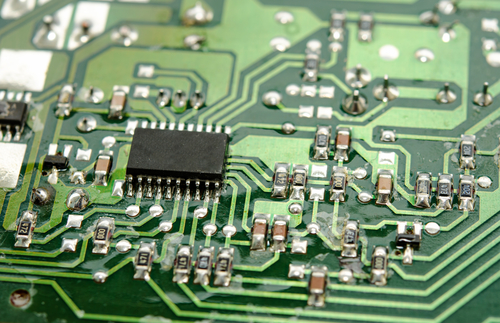
Circuit Board Components and Circuit Substrate
Overview of Common Components
Printed circuit boards (PCBs) host a variety of electronic components, each serving a specific function within the circuit. Common components found on PCBs include:
- Resistors: Control the flow of electrical current by providing resistance.
- Capacitors: Store and release electrical energy, used for filtering and smoothing signals.
- Inductors: Store energy in a magnetic field, often used in filtering and power supply applications.
- Diodes: Allow current to flow in one direction only, protecting circuits from reverse polarity.
- Transistors: Act as switches or amplifiers in electronic circuits.
- Integrated Circuits (ICs): Complex circuits with multiple functions, often the brain of an electronic device.
- Connectors: Provide connections between different PCBs or external devices.
- LEDs (Light Emitting Diodes): Indicate the status of the circuit or provide illumination.
- Switches: Allow the user to control the flow of current within the circuit.
Role of the Substrate in Component Placement and Performance
The circuit substrate plays a critical role in the placement and performance of these components. The substrate not only supports the components mechanically but also affects their electrical performance. Here’s how the substrate influences various aspects of the PCB:
- Thermal Management: Substrates like metal core PCBs (MCPCBs) help dissipate heat, ensuring components operate within safe temperature ranges. Effective thermal management is crucial for the longevity and reliability of components.
- Electrical Insulation: The substrate provides electrical insulation between conductive layers, preventing short circuits and ensuring signal integrity.
- Mechanical Support: A rigid substrate maintains the structural integrity of the PCB, allowing for secure mounting and placement of components. Flexible substrates, such as polyimide, enable the PCB to bend and fit into compact or irregularly shaped spaces.
- Signal Performance: High-frequency applications require substrates with low dielectric constants and low loss tangents, like Teflon or ceramic, to maintain signal integrity and reduce transmission losses.
- Component Density: Multi-layer substrates allow for higher component density by providing multiple layers for routing connections, essential for complex and compact electronic devices.
Solder Mask and Silkscreen Layers
Solder Mask: The solder mask is a protective layer applied over the copper traces of a PCB. It prevents accidental solder bridges from forming during assembly and protects the copper from oxidation and environmental damage. The solder mask also helps in:
- Improving the Insulation: It prevents short circuits by covering the conductive paths, leaving only the pads and vias exposed for soldering.
- Enhancing Durability: It adds an extra layer of protection against mechanical damage and corrosion.
- Aesthetic Appearance: The solder mask gives the PCB its characteristic green (or other colors) finish, enhancing the overall look of the board.
Silkscreen Layers: The silkscreen layer is used to print labels and markings on the PCB. It provides essential information for assembly, testing, and troubleshooting, such as:
- Component Identifiers: Labels for resistors, capacitors, ICs, and other components, which help in the accurate placement and orientation of parts during assembly.
- Test Points: Markings that indicate where to measure voltages or signals during testing and debugging.
- Manufacturer Logos and Part Numbers: Information that helps in tracking and identifying the PCB, especially in mass production.
The circuit substrate is fundamental to the functionality and reliability of a PCB. It influences component performance, thermal management, and overall durability. The solder mask and silkscreen layers further enhance the board’s functionality by protecting the circuit and providing critical information for assembly and maintenance.
Electrical Properties of Circuit Boards and Circuit Substrate
Conductivity and Insulation
Conductivity: The conductivity of a circuit substrate refers to its ability to conduct electric current. In PCBs, this is primarily managed by the copper traces and pads embedded on the substrate. Copper is highly conductive, making it an ideal material for creating the intricate pathways needed for electronic circuits. The circuit substrate itself, however, is typically an insulator to ensure that the conductive pathways remain distinct and do not short circuit.
- Copper Thickness: The thickness of the copper layers can affect the overall conductivity of the PCB. Thicker copper layers can handle higher current loads and improve the board’s durability and performance.
Insulation: The insulating properties of the circuit substrate are crucial for preventing unwanted electrical conduction between different conductive layers and components. Effective insulation ensures the proper functioning of the circuit by maintaining signal integrity and preventing short circuits.
- Materials: Common insulating materials include FR4 (fiberglass epoxy), ceramics, and polyimides. These materials provide excellent electrical insulation while supporting the mechanical structure of the PCB.
Dielectric Constant
The dielectric constant (Dk) of a circuit substrate material is a measure of its ability to store electrical energy in an electric field. It significantly impacts the signal speed and the impedance of the PCB.
- Low Dielectric Constant: Substrates with a low dielectric constant, such as Teflon and certain ceramics, are preferred for high-frequency applications. A lower Dk value reduces signal loss and dispersion, making it ideal for RF and microwave circuits.
- High Dielectric Constant: Materials with higher dielectric constants are used in applications where miniaturization is crucial, as they can store more energy in a smaller volume. However, they may introduce more signal delay and loss.
Thermal Conductivity
Thermal conductivity refers to the ability of a circuit substrate to conduct heat away from the components. Effective thermal management is essential for maintaining the performance and longevity of electronic devices, particularly in high-power and high-density circuits.
- High Thermal Conductivity Materials: Metal core PCBs (MCPCBs) with aluminum or copper cores are used in applications that require efficient heat dissipation, such as LED lighting and power electronics. These substrates can transfer heat away from hot spots more effectively than traditional FR4.
- Ceramic Substrates: Ceramic materials like alumina (Al2O3) and aluminum nitride (AlN) offer high thermal conductivity while maintaining excellent electrical insulation. These substrates are suitable for high-frequency and high-power applications, providing both thermal management and signal integrity.
- Thermal Vias: Incorporating thermal vias in the PCB design can enhance heat dissipation. These vias connect the top and bottom layers, allowing heat to flow through the board more efficiently.
The electrical properties of a circuit substrate play a pivotal role in the performance of a PCB. Conductivity and insulation ensure that electrical signals are transmitted accurately and reliably, while the dielectric constant and thermal conductivity influence signal integrity and thermal management. Understanding these properties helps in selecting the right substrate material for specific applications, ultimately improving the efficiency and reliability of electronic devices.
Understanding AMB (Active Metal Brazed) Substrates and Circuit Substrate
Definition and Applications
Definition: Active Metal Brazed (AMB) substrates are a type of circuit substrate that incorporates a layer of active metal brazing on ceramics, such as aluminum oxide (Al2O3) or aluminum nitride (AlN). The brazing process involves bonding a thin layer of metal, typically copper, to the ceramic substrate using an active metal, such as titanium, which promotes adhesion between the metal and ceramic. This creates a robust, thermally conductive, and electrically insulating substrate ideal for high-performance electronic applications.
Applications: AMB substrates are employed in various applications where high thermal conductivity and reliable electrical insulation are paramount. Typical applications include:
- Power Electronics: AMB substrates are widely used in power modules for electric vehicles (EVs), renewable energy systems, and industrial drives due to their ability to handle high power densities and dissipate heat efficiently.
- LED Technology: In high-power LED lighting, AMB substrates provide excellent thermal management, ensuring long life and consistent performance of the LEDs.
- RF and Microwave Devices: The high thermal conductivity and low dielectric loss of AMB substrates make them suitable for high-frequency applications, including RF amplifiers and microwave communication systems.
- Medical Devices: AMB substrates are used in medical electronics that require high reliability and thermal performance, such as imaging systems and diagnostic equipment.
Benefits over Traditional Substrates
Thermal Conductivity: One of the most significant advantages of AMB substrates over traditional substrates like FR4 or even standard ceramics is their superior thermal conductivity. The copper layer bonded to the ceramic efficiently conducts heat away from high-power components, reducing thermal stress and improving the overall reliability and lifespan of the device.
Mechanical Strength: The active metal brazing process creates a strong bond between the copper and ceramic layers, enhancing the mechanical strength of the substrate. This robustness is particularly beneficial in applications subjected to mechanical stress and vibration, such as automotive and aerospace electronics.
Electrical Performance: AMB substrates provide excellent electrical insulation while maintaining high thermal conductivity. This combination is critical for high-power and high-frequency applications where maintaining signal integrity and managing heat dissipation are essential.
Miniaturization: The efficient thermal management capabilities of AMB substrates allow for the design of smaller, more compact electronic devices. By effectively dissipating heat, these substrates enable higher component densities without the risk of overheating, supporting the trend towards miniaturization in electronics.
Reliability: The strong metallurgical bond between the copper and ceramic layers in AMB substrates results in high reliability and durability, even under extreme operating conditions. This makes AMB substrates ideal for applications requiring long-term stability and performance.
Chemical Resistance: Ceramic materials used in AMB substrates, such as aluminum oxide and aluminum nitride, offer excellent resistance to chemicals and environmental factors. This makes them suitable for use in harsh environments where traditional substrates might degrade.
AMB substrates represent a significant advancement in circuit substrate technology. Their superior thermal conductivity, mechanical strength, electrical performance, and reliability make them an excellent choice for high-power, high-frequency, and high-reliability applications. Understanding the benefits and applications of AMB substrates helps in selecting the appropriate material for advanced electronic designs, ultimately enhancing the performance and longevity of the devices.
Substrate Materials in Integrated Circuits (ICs) vs. PCBs and Circuit Substrate
Differences in Materials and Manufacturing Processes
Materials:
- Integrated Circuits (ICs):
- Silicon: The most common substrate material for ICs is silicon. Silicon wafers serve as the base for semiconductor devices, offering excellent electrical properties and compatibility with established manufacturing processes.
- Gallium Arsenide (GaAs): Used in high-frequency and optoelectronic applications due to its superior electron mobility and direct bandgap properties.
- Silicon Carbide (SiC) and Gallium Nitride (GaN): These materials are used in high-power and high-temperature applications, offering higher thermal conductivity and greater efficiency than silicon.
- Sapphire and Silicon on Insulator (SOI): Used in specific high-performance and radiation-resistant applications.
- Printed Circuit Boards (PCBs):
- FR4 (Fiberglass Epoxy): The most common PCB substrate material, providing a good balance of mechanical strength, thermal resistance, and cost-effectiveness.
- Metal Core (MCPCB): Utilized for enhanced thermal management, incorporating a metal core (usually aluminum or copper) to dissipate heat more effectively.
- Ceramics (Alumina, Aluminum Nitride): Employed in high-frequency and high-power applications due to their excellent thermal and electrical properties.
- Polyimide: Used for flexible PCBs, offering high thermal stability and flexibility.
- Teflon (PTFE), CEM-1, and CEM-3: Used in specialized applications requiring unique dielectric properties or cost advantages.
Manufacturing Processes:
- Integrated Circuits (ICs):
- Photolithography: The process of transferring intricate circuit patterns onto silicon wafers using light-sensitive photoresist materials.
- Doping: Introducing impurities into the silicon to modulate its electrical properties, creating p-type or n-type semiconductors.
- Etching and Deposition: Removing material to create the desired structures and depositing layers of different materials to build the circuit.
- Chemical Mechanical Planarization (CMP): A process to ensure the wafer surface is flat and smooth for subsequent layers.
- Printed Circuit Boards (PCBs):
- Layer Lamination: Multiple layers of substrate material and copper are laminated together to form multi-layer PCBs.
- Drilling and Plating: Creating vias and through-holes for electrical connections between layers and plating them with conductive materials.
- Etching: Removing unwanted copper to create the desired circuit patterns.
- Solder Mask and Silkscreen Application: Adding protective layers and markings to the PCB.
Application-specific Design Considerations
Integrated Circuits (ICs):
- Miniaturization: IC design focuses on packing more functionality into smaller areas. Substrate materials like silicon enable the creation of highly dense and complex circuits.
- Power Consumption: Materials like SiC and GaN are chosen for their efficiency in high-power applications, reducing energy loss and improving performance.
- High-frequency Performance: GaAs and similar materials are used in RF and microwave applications due to their superior electron mobility and high-frequency characteristics.
- Thermal Management: IC substrates must efficiently dissipate heat to prevent performance degradation and ensure reliability.
Printed Circuit Boards (PCBs):
- Component Density: Multi-layer PCBs with advanced substrate materials allow for higher component densities, crucial for complex and compact electronic designs.
- Thermal Management: MCPCBs and ceramic substrates are selected for their thermal conductivity in applications where heat dissipation is critical.
- Flexibility: Polyimide substrates are used in applications requiring flexible circuits, such as wearable devices and certain aerospace applications.
- Cost and Performance Balance: FR4 is commonly used due to its cost-effectiveness and satisfactory performance for a wide range of general-purpose applications.
- Signal Integrity: Substrates with low dielectric constants, like Teflon, are used in high-frequency applications to minimize signal loss and ensure integrity.
The choice of circuit substrate materials and manufacturing processes varies significantly between integrated circuits (ICs) and printed circuit boards (PCBs), driven by their distinct application requirements and performance criteria. Understanding these differences and the specific design considerations for each type of substrate helps optimize the performance, efficiency, and reliability of electronic devices across various applications.
Substrate Materials in Integrated Circuits (ICs) vs. PCBs and Circuit Substrate
Differences in Materials and Manufacturing Processes
Materials:
- Integrated Circuits (ICs):
- Silicon: The primary substrate material for ICs is silicon due to its excellent semiconductor properties. Silicon wafers serve as the base for constructing ICs, offering high electrical conductivity when doped and compatibility with well-established semiconductor manufacturing processes.
- Gallium Arsenide (GaAs): GaAs is used in high-frequency and optoelectronic applications because of its superior electron mobility and direct bandgap, which allows for efficient light emission and faster signal transmission.
- Silicon Carbide (SiC) and Gallium Nitride (GaN): These materials are employed in high-power and high-temperature applications. They offer higher thermal conductivity, greater efficiency, and the ability to operate at higher voltages and temperatures compared to silicon.
- Sapphire and Silicon on Insulator (SOI): Sapphire is used for high-performance and radiation-resistant applications, while SOI substrates are used to reduce parasitic capacitance, enhancing the performance of high-speed and low-power devices.
- Printed Circuit Boards (PCBs):
- FR4 (Fiberglass Epoxy): The most widely used PCB substrate, FR4 offers a balance of mechanical strength, thermal resistance, and cost-effectiveness. It is suitable for a broad range of applications from consumer electronics to industrial equipment.
- Metal Core (MCPCB): These substrates incorporate a metal core, usually aluminum or copper, to enhance thermal management. MCPCBs are used in applications where efficient heat dissipation is critical, such as LED lighting and power electronics.
- Ceramics (Alumina, Aluminum Nitride): Ceramic substrates are chosen for high-frequency and high-power applications due to their excellent thermal conductivity, low dielectric constant, and superior electrical insulation properties.
- Polyimide: Used for flexible PCBs, polyimide substrates offer high thermal stability and flexibility, making them ideal for applications where the PCB needs to bend or flex, such as in wearable devices and aerospace applications.
- Teflon (PTFE), CEM-1, and CEM-3: Teflon substrates are used in high-frequency applications due to their low dielectric constant and excellent electrical properties. CEM-1 and CEM-3 are used as cost-effective alternatives to FR4 in less demanding applications.
Manufacturing Processes:
- Integrated Circuits (ICs):
- Photolithography: This process involves transferring intricate circuit patterns onto silicon wafers using light-sensitive photoresist materials. It is critical for defining the small and precise features of ICs.
- Doping: Introducing impurities into silicon to create regions of p-type and n-type semiconductors, essential for forming the basic building blocks of ICs such as transistors.
- Etching and Deposition: Etching removes unwanted material to create the desired structures, while deposition adds layers of various materials to build the complex multi-layer structures of ICs.
- Chemical Mechanical Planarization (CMP): This process ensures a flat and smooth wafer surface, which is crucial for the subsequent layers’ precision and performance.
- Printed Circuit Boards (PCBs):
- Layer Lamination: Multi-layer PCBs are created by laminating several layers of substrate material and copper together. This process allows for the creation of complex and high-density circuit designs.
- Drilling and Plating: Vias and through-holes are drilled into the PCB to create electrical connections between layers, and these holes are then plated with conductive material to ensure reliable connections.
- Etching: Copper is etched away to leave behind the desired circuit patterns. This is typically done using a chemical process that removes unwanted copper from the PCB.
- Solder Mask and Silkscreen Application: A protective solder mask is applied to prevent short circuits and protect the copper traces. Silkscreen printing adds labels and markings to assist in component placement and circuit identification.
Application-specific Design Considerations
Integrated Circuits (ICs):
- Miniaturization: ICs require substrates that allow for extremely dense packing of transistors and other components. Silicon substrates enable the creation of highly integrated and compact circuits, which are essential for modern electronics.
- Power Consumption: IC designs often prioritize low power consumption, especially in battery-operated devices. Substrates like SiC and GaN are used in high-power applications due to their efficiency and ability to operate at higher voltages and temperatures.
- High-frequency Performance: Materials such as GaAs are chosen for high-frequency and RF applications due to their superior electron mobility, which allows for faster signal transmission and higher performance.
- Thermal Management: Efficient heat dissipation is crucial in ICs to maintain performance and reliability. Advanced substrates like SiC and GaN offer high thermal conductivity, which helps manage heat in high-power devices.
Printed Circuit Boards (PCBs):
- Component Density: Multi-layer PCBs allow for higher component densities by providing multiple layers for routing connections. This is crucial for complex and compact electronic designs, such as smartphones and computers.
- Thermal Management: Effective heat dissipation is vital in PCBs, particularly in high-power applications. Substrates like MCPCBs and ceramics are chosen for their superior thermal management properties, helping to prevent overheating and improve reliability.
- Flexibility: In applications requiring flexible circuits, such as wearable electronics and certain aerospace components, polyimide substrates are preferred due to their flexibility and high thermal stability.
- Cost and Performance Balance: FR4 is commonly used for its cost-effectiveness and satisfactory performance in a wide range of applications. It provides a good balance between cost, mechanical strength, and thermal resistance.
- Signal Integrity: Substrates with low dielectric constants, such as Teflon, are used in high-frequency applications to minimize signal loss and ensure signal integrity. These materials are critical for RF and microwave circuits where maintaining signal fidelity is essential.
The selection of substrate materials and manufacturing processes for ICs and PCBs is driven by their distinct application requirements and performance criteria. While ICs prioritize miniaturization, power efficiency, and high-frequency performance, PCBs focus on component density, thermal management, and flexibility. Understanding these differences is essential for optimizing the performance, efficiency, and reliability of electronic devices across various applications.
DBC (Direct Bonded Copper) Substrates and Circuit Substrate
Definition and Properties
Definition: Direct Bonded Copper (DBC) substrates are a type of circuit substrate that consists of a ceramic base, typically aluminum oxide (Al2O3) or aluminum nitride (AlN), onto which a layer of copper is directly bonded. The bonding process involves a high-temperature oxidation and reduction technique that creates a strong, metallurgical bond between the copper and the ceramic. This results in a highly reliable, thermally conductive, and electrically insulating substrate.
Properties:
- High Thermal Conductivity: DBC substrates provide excellent thermal management due to the direct bonding of copper to a ceramic material. Aluminum nitride-based DBC substrates offer particularly high thermal conductivity, making them ideal for applications requiring efficient heat dissipation.
- Electrical Insulation: The ceramic base of DBC substrates offers superior electrical insulation, which is critical for maintaining the integrity of electronic circuits and preventing short circuits.
- Mechanical Strength: The direct bonding process results in a robust and durable substrate capable of withstanding mechanical stresses and thermal cycling, enhancing the reliability and longevity of electronic devices.
- High Current Carrying Capacity: The thick copper layers (often ranging from 0.3 to 0.5 mm) can carry high currents, making DBC substrates suitable for power-intensive applications.
- Thermal Expansion Compatibility: The thermal expansion coefficients of DBC substrates are closely matched to those of semiconductor materials like silicon and silicon carbide. This minimizes thermal stress and improves the performance and reliability of power modules.
Applications in Power Electronics
Power Modules: DBC substrates are extensively used in power modules, which are critical components in power electronics systems. These modules are found in a variety of applications, including:
- Electric Vehicles (EVs): Power modules in EVs use DBC substrates to manage the high power levels and heat generated by the drive electronics. The excellent thermal conductivity of DBC substrates helps maintain optimal operating temperatures, improving efficiency and reliability.
- Renewable Energy Systems: Inverters and converters in solar and wind energy systems benefit from the high current carrying capacity and thermal management properties of DBC substrates. These substrates ensure efficient energy conversion and long-term stability.
- Industrial Drives: Motor drives and industrial automation systems use power modules with DBC substrates to handle high currents and manage heat dissipation effectively, ensuring consistent performance and durability.
LED Lighting: High-power LED lighting applications use DBC substrates to manage the significant heat generated by the LEDs. Efficient thermal management provided by DBC substrates enhances the lifespan and performance of LED lighting systems.
RF and Microwave Devices: The low dielectric loss and high thermal conductivity of DBC substrates make them suitable for RF and microwave applications, where signal integrity and thermal management are critical. These devices benefit from the robust properties of DBC substrates to maintain high performance under demanding conditions.
Medical Electronics: In medical devices, such as imaging equipment and diagnostic instruments, DBC substrates offer reliability and efficient thermal management, which are essential for maintaining accuracy and performance over extended periods.
Power Supply Units (PSUs): Power supply units in various electronic devices use DBC substrates to handle high power levels and ensure stable operation. The thermal and electrical properties of DBC substrates contribute to the overall efficiency and reliability of PSUs.
DBC substrates are a crucial component in power electronics due to their excellent thermal conductivity, electrical insulation, and mechanical strength. Their ability to handle high currents and manage heat effectively makes them indispensable in a wide range of high-power and high-reliability applications. Understanding the properties and applications of DBC substrates helps in selecting the right materials for optimizing the performance and durability of power electronic systems.
PCB Manufacturing Process and Circuit Substrate
Steps in PCB Fabrication
1. Design and Layout: The PCB fabrication process begins with designing the circuit schematic and layout using computer-aided design (CAD) software. Designers determine the placement of components, routing of traces, and layer stackup based on the circuit requirements.
2. Substrate Material Preparation: The chosen substrate material, such as FR4, is prepared by cutting it into appropriate sizes based on the PCB design. The substrate may undergo surface treatments, such as cleaning and etching, to ensure proper adhesion of copper and other layers.
3. Copper Cladding: In this step, a thin layer of copper foil is laminated onto the substrate material. The copper foil adheres to the substrate surface through heat and pressure, forming the conductive layer for the PCB traces.
4. Photoresist Application: A layer of photoresist material is applied over the copper-clad substrate. Photoresist is sensitive to ultraviolet light and serves as a protective layer during the etching process.
5. Imaging and Etching: The PCB design is transferred onto the photoresist layer using a photomask and ultraviolet light exposure. Areas not covered by the design are exposed and chemically etched away, leaving behind the desired copper traces.
6. Layer Alignment and Lamination: For multi-layer PCBs, individual copper-clad substrates with etched traces are aligned and laminated together. The layers are bonded under heat and pressure to form a single, multi-layered PCB stackup.
7. Drilling: Small holes, called vias, are drilled into the PCB to establish electrical connections between different layers. Through-holes are also drilled for mounting components and providing access to external connections.
8. Plating: After drilling, the vias and through-holes are plated with a conductive material, typically copper, to ensure reliable electrical connections between layers and components.
9. Solder Mask Application: A solder mask layer is applied over the PCB surface, covering the copper traces and leaving only the component pads and vias exposed. The solder mask protects the copper traces from oxidation and facilitates soldering during assembly.
10. Silkscreen Printing: Labels, markings, and component identifiers are printed onto the PCB surface using a silkscreen printing process. This provides essential information for component placement, assembly, and troubleshooting.
11. Surface Finish: A surface finish is applied to the exposed copper surfaces to improve solderability, prevent oxidation, and enhance the PCB’s overall durability. Common surface finishes include hot air solder leveling (HASL), electroless nickel immersion gold (ENIG), and immersion tin.
12. Electrical Testing: The fabricated PCB undergoes electrical testing to ensure that all traces, vias, and connections meet the design specifications and function as intended. Automated testing equipment is used to detect any defects or faults in the PCB.
Key Manufacturers and Industry Leaders
1. TTM Technologies, Inc.: TTM Technologies is one of the largest PCB manufacturers globally, offering a comprehensive range of PCB fabrication services for various industries, including aerospace, automotive, and telecommunications.
2. Nippon Mektron, Ltd.: Nippon Mektron is a leading Japanese manufacturer of high-quality PCBs for automotive electronics, consumer electronics, and industrial applications. The company specializes in advanced PCB technologies, including high-density interconnects (HDIs) and flexible PCBs.
3. Zhen Ding Technology Holding Limited: Zhen Ding Technology is a prominent PCB manufacturer based in Taiwan, known for its innovative solutions and advanced manufacturing capabilities. The company serves customers in the smartphone, tablet, and wearable device markets.
4. Unimicron Technology Corporation: Unimicron is a major player in the global PCB industry, offering a wide range of PCB products and services, including rigid, flexible, and rigid-flex PCBs. The company focuses on delivering high-quality, reliable PCB solutions to its customers worldwide.
5. Samsung Electro-Mechanics Co., Ltd.: Samsung Electro-Mechanics is a subsidiary of Samsung Group and a leading manufacturer of PCBs and electronic components. The company provides high-performance PCB solutions for smartphones, tablets, and other consumer electronics devices.
6. Ibiden Co., Ltd.: Ibiden is a Japanese company specializing in advanced PCB technologies and sustainable manufacturing practices. The company is known for its expertise in high-density interconnect (HDI) PCBs and environmentally friendly production processes.
7. AT&S Austria Technologie & Systemtechnik AG: AT&S is an Austrian PCB manufacturer with a global presence, offering a wide range of PCB products and services for various industries, including automotive, aerospace, and medical devices. The company is known for its high-quality, high-density PCB solutions.
8. Tripod Technology Corporation: Tripod Technology is a leading Taiwanese manufacturer of PCBs, specializing in high-density interconnect (HDI) and flexible PCBs. The company serves customers in the telecommunications, computing, and automotive industries.
Selection Criteria for Circuit Substrates and Circuit Substrate
Factors to Consider
1. Electrical Properties:
- Dielectric Constant (Dk): The dielectric constant of the substrate affects the speed and impedance of signals transmitted through the circuit. Lower Dk values are preferred for high-frequency applications to minimize signal loss.
- Conductivity: Substrates should provide adequate electrical insulation to prevent short circuits while allowing efficient conduction of electrical signals along traces and vias.
2. Thermal Management:
- Thermal Conductivity: High thermal conductivity is essential for dissipating heat generated by electronic components. Substrates with high thermal conductivity, such as metal core PCBs or DBC substrates, are preferred for power electronics and high-power applications.
- Coefficient of Thermal Expansion (CTE): Matching the CTE of the substrate with that of the components reduces mechanical stress and the risk of solder joint failure due to thermal cycling.
3. Mechanical Properties:
- Mechanical Strength: Substrates should have sufficient mechanical strength to support components and withstand handling during assembly and operation. Flexible substrates may be required for applications involving bending or flexing, such as wearable devices.
- Durability: Substrates should be resistant to environmental factors such as moisture, humidity, and mechanical shock to ensure long-term reliability.
Application-specific Requirements
1. Power Electronics:
- High Thermal Conductivity: Substrates with high thermal conductivity, such as DBC or metal core PCBs, are crucial for managing heat in power electronics applications like inverters, converters, and motor drives.
- High Current Carrying Capacity: Substrates should be capable of carrying high currents without excessive resistance or overheating. Thick copper layers and low-resistance materials are preferred.
2. High-Frequency Applications:
- Low Dielectric Loss: Substrates with low dielectric loss and low Dk values are essential for maintaining signal integrity and minimizing signal attenuation in high-frequency circuits, such as RF amplifiers and microwave communication systems.
- Uniform Dielectric Properties: Consistent dielectric properties across the substrate are necessary to ensure predictable signal propagation and impedance matching.
3. Aerospace and Automotive Electronics:
- Reliability: Substrates used in aerospace and automotive electronics must meet stringent reliability standards to withstand harsh environments, temperature extremes, and mechanical stress.
- High Temperature Operation: Substrates should be capable of operating reliably at elevated temperatures encountered in aerospace and automotive applications.
4. Consumer Electronics:
- Cost-effectiveness: Substrates for consumer electronics often prioritize cost-effectiveness while maintaining acceptable performance and reliability. FR4 and other standard substrates are commonly used for these applications.
- Miniaturization: Substrates that enable miniaturization and high component density are desirable for consumer electronics devices like smartphones, tablets, and wearables.
5. Medical Devices:
- Biocompatibility: Substrates used in medical devices must be biocompatible and safe for use in contact with the human body. Materials should be free from harmful chemicals and meet regulatory standards for medical device manufacturing.
- Reliability and Longevity: Medical devices require substrates with high reliability and long-term stability to ensure patient safety and consistent performance over extended periods.
Selecting the right circuit substrate involves considering various factors such as electrical, thermal, and mechanical properties, as well as application-specific requirements. Understanding these criteria helps engineers and designers choose substrates that optimize performance, reliability, and cost-effectiveness for their specific applications.
FAQs About Circuit Substrate
What is a substrate in circuits?
In the context of circuits, a substrate refers to the base material upon which electronic components and interconnections are fabricated. It provides mechanical support, electrical insulation, and a foundation for building electronic circuits. Substrates can vary widely in composition, ranging from traditional materials like fiberglass epoxy (FR4) used in printed circuit boards (PCBs) to advanced materials like silicon or gallium arsenide used in integrated circuits (ICs).
What is an electronic substrate?
An electronic substrate is a material used as the base or foundation for electronic components and circuits. It provides mechanical support and electrical insulation while facilitating the interconnection of various components. Electronic substrates can be rigid or flexible and are chosen based on factors such as electrical properties, thermal conductivity, mechanical strength, and application requirements.
What is the difference between IC substrate and PCB?
The main difference between an IC substrate and a PCB lies in their primary function and application:
- IC Substrate: An IC substrate, also known as a semiconductor substrate or chip carrier, serves as the base for mounting and interconnecting semiconductor devices such as integrated circuits (ICs) or chips. It provides electrical connections between the IC and the external circuitry while also dissipating heat generated by the IC. IC substrates are typically made of materials like silicon, ceramic, or laminate substrates designed specifically for semiconductor manufacturing processes.
- PCB (Printed Circuit Board): A PCB is a flat board made of insulating material (substrate) with conductive pathways (traces) etched or printed onto its surface. PCBs are used to mechanically support and electrically connect electronic components such as resistors, capacitors, and integrated circuits (ICs) to form functional electronic circuits. They are widely used in various electronic devices, ranging from consumer electronics to industrial equipment.
What is DBC substrate?
DBC stands for Direct Bonded Copper. DBC substrates are a type of circuit substrate commonly used in power electronics applications. They consist of a ceramic base, such as aluminum oxide (Al2O3) or aluminum nitride (AlN), onto which a layer of copper is directly bonded. DBC substrates offer high thermal conductivity, excellent electrical insulation, and mechanical strength, making them ideal for managing heat in power-intensive applications like inverters, converters, and motor drives.

