
What Is the UV Exposure Effect on the PCB Substrate
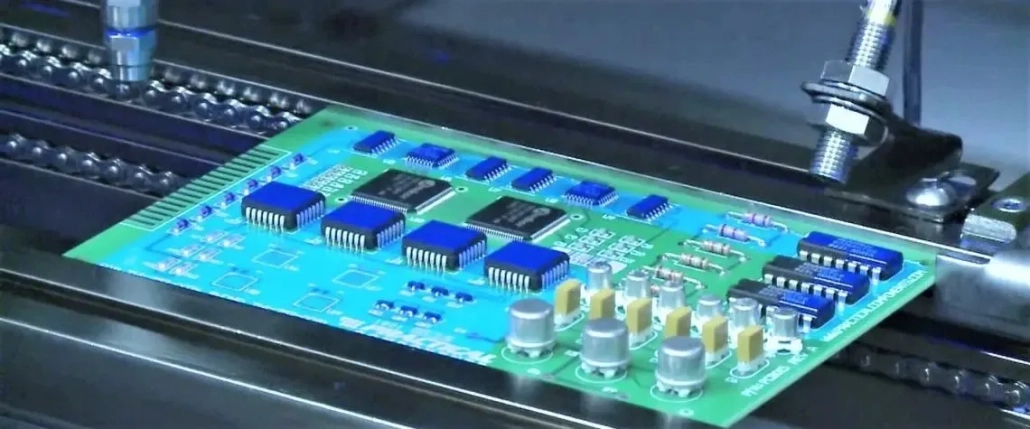
Printed Circuit Boards (PCBs) are the backbone of modern electronics, providing a platform for interconnecting electronic components to form functional devices. Their importance in electronic devices cannot be overstated, as they enable the efficient flow of electricity and data within intricate electronic systems. Within the PCB fabrication process, UV exposure plays a pivotal role. It serves as a critical step in defining the circuit patterns on the PCB substrate. Understanding what is the UV exposure effect on the PCB substrate is paramount for ensuring the accuracy and reliability of the final product. In this article, we delve into the intricate relationship between UV exposure and PCB substrates, exploring its implications and significance in electronic manufacturing.
UV Exposure Process in PCB Fabrication: Understanding the Impact on the PCB Substrate
In the intricate process of PCB fabrication, UV exposure stands as a crucial step, profoundly influencing the substrate. This step involves exposing the PCB substrate coated with a layer of photosensitive material, typically photoresist, to UV light. The UV light passes through a photomask, selectively curing the photoresist, thus defining the circuit patterns on the substrate.
Equipment Utilized for UV Exposure: The equipment used for UV exposure includes UV light sources, photomasks, and exposure chambers. UV light sources emit light at specific wavelengths suitable for curing the photoresist. Photomasks, containing the desired circuit patterns, allow precise control over the exposure process. Exposure chambers provide a controlled environment for uniform exposure across the PCB substrate.
Importance of UV Exposure for Precision Circuit Patterns: The UV exposure step is critical for achieving PCBs with accurate and precise circuit patterns. The controlled exposure ensures that the photoresist is cured only in areas where circuit traces are intended, while leaving other areas unaffected. This precision is essential for the functionality and reliability of the final electronic device. Understanding what is the UV exposure effect on the PCB substrate is fundamental for optimizing this step to achieve high-quality PCBs with intricate circuitry.
UV Exposure Effect on PCB Substrate: Unraveling Its Impact
In the realm of PCB fabrication, the effect of UV exposure on the substrate is profound, shaping its intricacies in significant ways. This section delves into the intricate details of this effect, shedding light on its various facets.
Detailed Exploration of UV Exposure’s Influence: UV exposure exerts a transformative effect on the PCB substrate, primarily through its interaction with the photoresist layer. Upon exposure to UV light, the photosensitive molecules within the photoresist undergo a chemical reaction, causing them to either harden or soften depending on the type of photoresist used. This process essentially defines the areas where the circuit traces and features will be formed on the substrate.
Explanation of UV Light Interaction with Photoresist Layer: The interaction between UV light and the photoresist layer is governed by the principles of photochemistry. When UV light hits the photoresist-coated substrate, it initiates a photopolymerization reaction, causing the molecules in the photoresist to cross-link and form a stable polymer network. This reaction occurs selectively in areas exposed to UV light, as dictated by the pattern on the photomask. Consequently, the unexposed areas remain soluble and are subsequently removed during the development process, revealing the desired circuit patterns.
Role of UV Exposure in Defining Circuit Traces and Features: UV exposure plays a pivotal role in defining the precise circuit traces and features on the PCB substrate. By selectively curing the photoresist, UV light essentially acts as a stencil, transferring the intricate design from the photomask onto the substrate. This step is crucial for ensuring the accuracy and fidelity of the circuit patterns, ultimately determining the functionality and reliability of the final electronic device. Understanding what is the UV exposure effect on the PCB substrate is paramount for optimizing this process and achieving high-quality PCBs with intricate circuitry.
Light Sensitivity of PCBs: Understanding Its Impact
The light sensitivity of PCBs is a critical aspect that warrants careful consideration in electronic design and fabrication processes. This section delves into the nuances of PCB light sensitivity and its implications on performance and longevity.
Investigation into PCB Light Sensitivity: PCBs exhibit varying degrees of light sensitivity, depending on factors such as the materials used in their construction and the manufacturing processes employed. Understanding what is the UV exposure effect on the PCB substrate sheds light on the intricacies of its light sensitivity.
Factors Influencing PCB Light Sensitivity: Several factors influence the light sensitivity of PCB materials. The composition of the substrate, particularly the presence of photoactive components such as photoresist, significantly impacts its sensitivity to UV light. Additionally, the thickness and quality of the protective coating layers applied to the PCB can influence its vulnerability to light-induced degradation.
Effects of Prolonged Light Exposure on PCB Performance and Longevity: Prolonged exposure to light can have detrimental effects on the performance and longevity of PCBs. UV radiation, in particular, can cause photochemical degradation of the substrate materials, leading to changes in electrical properties, degradation of solder mask integrity, and increased risk of delamination. Furthermore, excessive light exposure can accelerate aging processes, ultimately compromising the reliability and lifespan of the electronic device.
Understanding the light sensitivity of PCBs is crucial for mitigating potential risks and ensuring the longevity and reliability of electronic systems. By considering the effects of light exposure during the design and manufacturing stages, engineers can implement strategies to protect PCBs from undue damage and degradation, ultimately enhancing the performance and durability of electronic devices.
Wavelength of UV for Photoresist: Optimizing Exposure for PCB Substrate
Understanding what is the UV exposure effect on the PCB substrate necessitates a comprehensive examination of the UV wavelengths utilized in the PCB fabrication process. This section provides insights into the intricacies of UV light wavelengths, their significance in photoresist exposure, and common UV light sources employed in PCB manufacturing.
Explanation of Specific UV Light Wavelengths: UV light used in PCB fabrication typically falls within the ultraviolet spectrum, encompassing wavelengths ranging from approximately 200 to 400 nanometers (nm). Within this range, specific wavelengths are tailored to match the sensitivity of the photoresist material employed. For instance, deep UV (DUV) light sources emitting wavelengths in the range of 240 to 365 nm are commonly utilized for high-resolution patterning of advanced photoresists.
Importance of Selecting Appropriate UV Wavelength: The selection of the appropriate UV wavelength is paramount in achieving precise and reliable photoresist exposure. Different photoresist materials exhibit varying degrees of sensitivity to UV light, with optimal exposure conditions dictated by the absorption spectra of the photoactive components. By matching the UV wavelength to the absorption peak of the photoresist, engineers can ensure efficient photopolymerization and accurate pattern transfer onto the PCB substrate.
Overview of Common UV Light Sources: Several UV light sources find application in PCB manufacturing, each emitting specific wavelengths tailored to suit different photoresist formulations and process requirements. Mercury vapor lamps, commonly used in conventional UV exposure systems, emit broadband UV radiation covering a range of wavelengths suitable for general-purpose photoresists. Alternatively, advanced UV sources such as excimer lasers and UV LED arrays offer precise control over wavelength and intensity, enabling fine-tuning of exposure parameters for demanding applications requiring high resolution and throughput.
By understanding the nuances of UV light wavelengths and their interaction with photoresist materials, engineers can optimize the exposure process to achieve superior patterning fidelity and overall PCB performance. Selecting the appropriate UV light source and wavelength tailored to the specific requirements of the PCB design and fabrication process is essential for realizing high-quality, reliable electronic devices.
Applications and Considerations: Expanding the Reach of UV Exposure on PCB Substrate
Exploring what is the UV exposure effect on the PCB substrate reveals a plethora of applications and considerations that extend beyond mere photoresist exposure. This section delves into the diverse realms where UV exposure finds utility in PCB fabrication, considerations for optimizing UV exposure processes, and emerging trends in UV exposure technology.
Applications of UV Exposure Beyond Photoresist: UV exposure serves as a versatile tool in PCB fabrication, with applications extending beyond photoresist exposure. UV-curable solder masks, for instance, leverage UV radiation to achieve rapid curing, enhancing the efficiency of the solder mask application process. Additionally, UV exposure enables the fabrication of flexible PCBs through the photopolymerization of flexible substrates, facilitating the development of innovative electronic devices with bendable form factors.
Considerations for Optimizing UV Exposure Processes: Optimizing UV exposure processes entails careful consideration of various factors, including PCB design complexity, substrate material properties, and desired circuit resolution. Fine-tuning exposure parameters such as UV intensity, exposure time, and wavelength selection is crucial for achieving optimal patterning fidelity and minimizing the risk of overexposure or underexposure. Furthermore, substrate surface preparation and post-exposure processing steps play pivotal roles in ensuring uniform photoresist coverage and pattern definition across the PCB substrate.
Future Trends and Advancements in UV Exposure Technology: The future of UV exposure technology in PCB manufacturing holds promise for further advancements aimed at enhancing precision, efficiency, and sustainability. Emerging trends include the integration of UV LED arrays for energy-efficient and environmentally friendly exposure systems, as well as the development of novel photoresist materials with enhanced sensitivity and resolution capabilities. Furthermore, advancements in photomask fabrication techniques, such as direct laser writing and multi-beam lithography, are poised to revolutionize the patterning process, enabling the realization of submicron-scale features on PCB substrates.
By leveraging UV exposure beyond traditional photoresist applications, optimizing exposure processes for diverse PCB designs and materials, and embracing emerging trends in UV exposure technology, manufacturers can unlock new possibilities for innovation and excellence in PCB fabrication. Understanding what is the UV exposure effect on the PCB substrate serves as a cornerstone for navigating these opportunities and shaping the future landscape of electronic device manufacturing.
FAQs About What Is the UV Exposure Effect on the PCB Substrate
The UV exposure for PCB (Printed Circuit Board) involves exposing the PCB substrate coated with a layer of photosensitive material, typically photoresist, to UV light. This process defines circuit patterns on the substrate.
The exposure process in PCB involves using UV light to selectively cure the photoresist layer on the PCB substrate. This step is crucial for creating accurate and precise circuit patterns.
Yes, PCBs are light-sensitive, particularly to UV light. Prolonged exposure to light, especially UV radiation, can affect the performance and longevity of PCBs, causing photochemical degradation and other issues.
The wavelength of UV light used for photoresist exposure in PCB fabrication typically ranges from approximately 200 to 400 nanometers (nm). Specific wavelengths are selected based on the sensitivity of the photoresist material to ensure optimal curing and pattern transfer onto the PCB substrate.


发表评论
Want to join the discussion?Feel free to contribute!