
Substrate in Electronics: Types and Functions
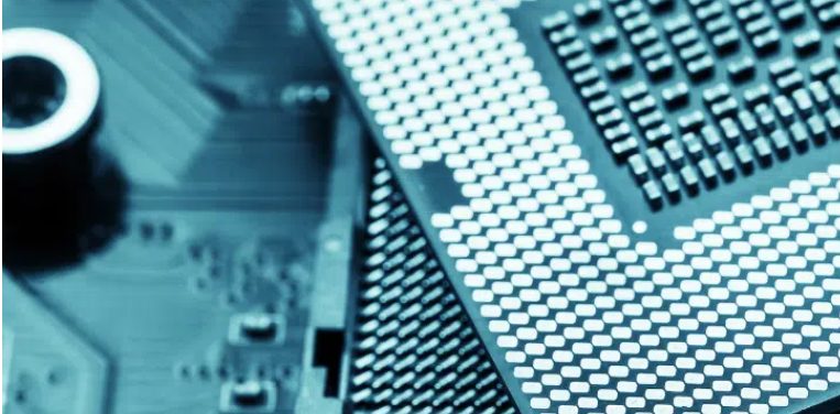
In electronics, a substrate refers to a fundamental material on which electronic components or circuits are fabricated or mounted. It provides a solid base that supports and interconnects various components, enabling their function within electronic devices. Substrates range from semiconductors like silicon and gallium arsenide to specialized materials such as ceramics and polymers used in printed circuit boards (PCBs).
The role of substrates in electronics is crucial, as they not only provide mechanical support but also facilitate electrical connections and thermal management. They influence the performance, reliability, and manufacturability of electronic systems, affecting everything from signal integrity to power dissipation. Understanding substrate properties and choosing the right material is essential for optimizing the functionality and longevity of electronic devices in diverse applications.
Types of Substrates
Semiconductor Substrates
Silicon: Silicon is the most widely used semiconductor substrate in electronics due to its abundance and well-understood manufacturing processes. It serves as the foundation for integrated circuits (ICs), microprocessors, and memory chips.
Gallium Arsenide: Gallium arsenide (GaAs) substrates are valued for their high electron mobility, making them suitable for high-frequency applications like RF (radio frequency) and microwave devices.
Silicon Carbide: Silicon carbide (SiC) substrates offer superior thermal conductivity and power handling capabilities, making them ideal for high-power electronics, such as power supplies and electric vehicles.
Printed Circuit Board (PCB) Substrates
FR4: FR4 is a flame-retardant epoxy laminate material used extensively in PCB manufacturing for its affordability, electrical insulation properties, and ease of fabrication.
CEM-1: CEM-1 (Composite Epoxy Material) is another type of PCB substrate known for its cost-effectiveness and moderate electrical and mechanical properties, suitable for single-layer and double-layer PCBs.
Polyimide: Polyimide substrates provide excellent thermal stability and flexibility, making them ideal for flexible PCBs used in applications requiring high reliability and resistance to harsh environments.
Ceramic Substrates
Alumina: Alumina (Al2O3) substrates offer high mechanical strength, excellent thermal conductivity, and electrical insulation properties, making them suitable for power electronics, LEDs, and semiconductor packaging.
Aluminum Nitride: Aluminum nitride (AlN) substrates exhibit high thermal conductivity, low coefficient of thermal expansion, and good dielectric properties, making them ideal for high-power and high-frequency electronic applications, such as LED modules and microwave circuits.
Specialized Substrates
DBC (Direct Bonded Copper) Substrates
Definition and Applications: Direct Bonded Copper (DBC) substrates are specialized structures where a copper layer is directly bonded to a ceramic substrate, typically alumina or aluminum nitride. This configuration provides excellent thermal conductivity and mechanical stability, making DBC substrates ideal for power electronic modules, such as insulated gate bipolar transistors (IGBTs), where efficient heat dissipation is critical.
Manufacturing Process: The manufacturing of DBC substrates involves several steps:
- Cleaning and Preparation: Ceramic and copper surfaces are meticulously cleaned to ensure proper bonding.
- Bonding: The copper foil is bonded to the ceramic substrate under high pressure and temperature in a controlled atmosphere.
- Post-processing: After bonding, the substrate undergoes machining, polishing, and sometimes coating to meet specific dimensional and surface finish requirements.
- Integration: Electronic components are mounted on the substrate using techniques like soldering or wire bonding.
AMB (Active Metal Brazed) Substrates
Definition and Applications: Active Metal Brazed (AMB) substrates consist of a ceramic material bonded to a metal layer using a brazing process involving active metals like titanium or tantalum. AMB substrates are valued for their high reliability in demanding environments and find applications in aerospace, automotive sensors, and high-power electronics.
Manufacturing Process: The manufacturing process of AMB substrates typically includes:
- Surface Preparation: Similar to DBC substrates, ceramic and metal surfaces are cleaned and prepared for bonding.
- Brazing: Active metal brazing involves heating the assembly to a specific temperature where the active metal forms a metallurgical bond between the ceramic and metal layers.
- Cooling and Inspection: After brazing, the substrate is slowly cooled to relieve stresses and then inspected for defects such as voids or cracks.
- Finishing: The substrate may undergo finishing processes such as machining or coating to achieve final dimensions and surface properties suitable for electronic assembly.
Both DBC and AMB substrates represent advanced technologies tailored to specific performance requirements in electronic and mechanical applications, offering enhanced thermal management and structural integrity compared to traditional substrates.
Substrate Materials
Common Materials
Silicon: Silicon substrates are widely used in semiconductor manufacturing due to their semiconductor properties, which allow for the fabrication of integrated circuits (ICs) and microelectromechanical systems (MEMS). Silicon offers excellent electrical properties and is compatible with standard semiconductor processes, making it indispensable in the electronics industry.
Alumina: Alumina (Al2O3) substrates are preferred for their high mechanical strength, excellent thermal conductivity, and good electrical insulation properties. They are commonly used in applications requiring robustness and reliability, such as in power electronics modules, LEDs, and semiconductor packaging.
Aluminum Nitride: Aluminum nitride (AlN) substrates exhibit exceptionally high thermal conductivity, low coefficient of thermal expansion, and excellent electrical insulation properties. These properties make AlN ideal for applications where efficient heat dissipation and electrical isolation are critical, such as in high-power electronics, microwave circuits, and LED modules.
Considerations for Choosing Substrate Materials
Thermal Conductivity: The thermal conductivity of a substrate material is crucial for efficiently dissipating heat generated by electronic components. Materials like aluminum nitride (AlN) and silicon carbide (SiC) offer high thermal conductivity, which helps in reducing thermal resistance and improving device performance.
Mechanical Strength: Substrates must provide adequate mechanical strength to support electronic components and withstand mechanical stresses during manufacturing, assembly, and operation. Ceramic materials such as alumina and aluminum nitride offer high mechanical strength, ensuring reliability and longevity in harsh operating conditions.
Electrical Insulation Properties: Electrical insulation is essential to prevent short circuits and ensure the proper functioning of electronic devices. Materials like alumina and polyimide offer excellent electrical insulation properties, maintaining electrical isolation between components and substrate layers.
Choosing the right substrate material involves balancing these properties based on the specific requirements of the application, such as operating temperature range, thermal management needs, mechanical robustness, and electrical performance. Each material’s characteristics play a critical role in determining the overall performance and reliability of electronic systems and devices.
Substrates in the Semiconductor Industry
Role of Substrates in Semiconductor Manufacturing
Epitaxial Growth: Substrates serve as the foundation for epitaxial growth processes, where thin layers of crystalline semiconductor materials are deposited onto the substrate’s surface. Epitaxy is crucial for creating the active regions of transistors and other semiconductor devices with precise crystal structures and electrical properties.
Thin Film Deposition: Substrates provide a platform for depositing thin films of materials such as oxides, nitrides, and metals through techniques like chemical vapor deposition (CVD) and physical vapor deposition (PVD). These thin films form essential components of semiconductor devices, including gate dielectrics, interconnects, and passivation layers.
Device Fabrication: Substrates play a pivotal role in the fabrication of semiconductor devices by providing a stable base for lithography, etching, doping, and metallization processes. These processes enable the creation of integrated circuits (ICs), diodes, transistors, and sensors with high precision and reliability.
Use of Substrates in Electronic Packaging
Types of Packaging: Substrates are integral to various electronic packaging techniques that protect and interconnect semiconductor devices. Common packaging types include:
- Dual in-line packages (DIP): Traditional packaging for integrated circuits with two parallel rows of leads.
- Ball Grid Array (BGA): Uses solder balls for electrical connections on the underside of the package.
- Chip-on-board (COB): Directly mounts semiconductor chips onto PCBs without encapsulation.
Thermal Management: Effective thermal management is critical in semiconductor devices to maintain optimal operating temperatures and prevent overheating. Substrates with high thermal conductivity, such as aluminum nitride (AlN) and silicon carbide (SiC), are used to enhance heat dissipation from active components. Techniques like heat sinks, thermal vias, and encapsulation materials help in efficiently managing thermal energy within electronic packages.
Substrates in the semiconductor industry not only support the manufacturing and performance of semiconductor devices but also play a vital role in ensuring reliability, thermal efficiency, and functionality in diverse electronic applications.
Substrate vs. PCB
Is Substrate the Same as PCB?
No, substrate and PCB (Printed Circuit Board) are not the same, although there is overlap in their functionality within electronic systems.
Definition and Structure of PCBs
PCB Definition: A PCB is a rigid or flexible board made of non-conductive substrate materials, typically fiberglass-reinforced epoxy (FR4) or polyimide, with conductive pathways etched or printed on its surface. These pathways, known as traces, provide electrical connections between electronic components mounted on the board.
PCB Structure:
- Substrate Layer: The base material (e.g., FR4 or polyimide) provides mechanical support and insulation.
- Conductive Layers: Copper foils are laminated onto the substrate and etched to create traces that interconnect components.
- Component Mounting Areas: Areas for soldering or attaching electronic components such as resistors, capacitors, and integrated circuits.
- Solder Mask: Non-conductive layer applied over the conductive traces to prevent short circuits and facilitate soldering.
- Silkscreen: Printed text and symbols for component placement and identification.
Role of Substrates within PCBs
Substrates within PCBs refer to the base material (e.g., FR4) on which conductive layers are deposited to form the circuitry. The substrate provides structural support for the PCB and determines its mechanical properties. It also influences the electrical performance of the board, including factors like signal integrity, impedance control, and thermal management.
Specifically:
- Mechanical Support: Substrates ensure the rigidity or flexibility of the PCB, depending on the application requirements.
- Dielectric Properties: Substrates act as electrical insulators between conductive layers, preventing short circuits and maintaining signal integrity.
- Thermal Management: Substrate materials with good thermal conductivity (e.g., metal core PCBs with aluminum or copper substrates) help dissipate heat from components, enhancing reliability and longevity.
Understanding the distinction between substrates and PCBs is crucial for designing and manufacturing electronic circuits that meet performance, reliability, and cost-efficiency criteria across various applications.
Substrate in Biology
Definition and Examples
What is a substrate in biology?
In biology, a substrate refers to the underlying surface or material on which an organism lives, grows, or interacts. It provides physical support and may also supply nutrients or other essential factors necessary for the organism’s survival and function.
Common Examples of Biological Substrates
Biological substrates vary widely across different ecosystems and organisms:
- Soil: Soil serves as a substrate for plants, providing anchorage, water, and essential nutrients for growth.
- Rocks and Coral Reefs: Substrates for marine organisms such as algae, corals, and mollusks, providing attachment points and habitats.
- Wood: Decomposing wood acts as a substrate for fungi and insects, facilitating nutrient cycling in forest ecosystems.
- Human Body Surfaces: Human skin and mucosal surfaces serve as substrates for the colonization of various microorganisms, forming diverse microbiomes crucial for health.
Understanding biological substrates is essential in ecology, microbiology, and environmental sciences, as they influence the distribution, diversity, and interactions of organisms within ecosystems. The characteristics of a substrate can determine which species thrive in a particular habitat, affecting ecosystem dynamics and biodiversity.
FAQs About substrate in electronics
A substrate material refers to the base material upon which electronic components or circuits are fabricated or mounted. This material provides structural support, electrical insulation, and thermal management capabilities depending on the application requirements. Common substrate materials include ceramics (like alumina and aluminum nitride), metals, and various types of polymers.
No, a substrate is not the same as a PCB (Printed Circuit Board). While a PCB includes a substrate layer as its base material (such as FR4 or polyimide), it also includes conductive pathways and components mounted on the substrate to form an electronic circuit.
In the semiconductor industry, a substrate typically refers to the base material upon which semiconductor devices are fabricated. This can include silicon wafers, which serve as the foundation for manufacturing integrated circuits (ICs), or specialized substrates like silicon carbide (SiC) or gallium arsenide (GaAs) used in high-frequency and power electronics.
Electronic packaging substrates refer to materials used to physically support and interconnect semiconductor devices within a package. These substrates must possess high thermal conductivity, good electrical insulation properties, and mechanical strength. Common substrate materials used in electronic packaging include ceramics such as alumina and aluminum nitride, as well as metal core PCBs (MCPCBs) using materials like aluminum or copper for improved thermal management.

