
Role of Quad Flat Pack Lead Frame in Packaging
Semiconductor packaging is crucial in electronics, as it protects and connects integrated circuits (ICs), enabling them to function properly within devices. Packaging shields ICs from environmental factors like moisture and heat, while providing electrical connections to the external system. As electronic devices evolve, the demand for advanced packaging solutions increases. One such solution is the Quad Flat Pack Lead Frame, a popular packaging type that features a flat, rectangular shape with leads extending from all four sides. Lead frames are vital in many semiconductor packages, ensuring precise and reliable interconnects for a variety of applications. They support the IC during assembly, ensuring its functionality and longevity in end devices, making them an essential part of modern electronics.
What is a Quad Flat Pack (QFP) and the Role of Quad Flat Pack Lead Frame in Semiconductor Packaging?
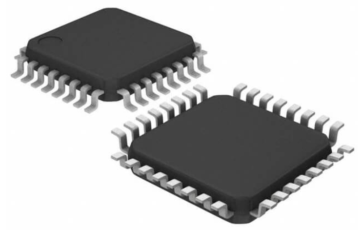
A Quad Flat Pack (QFP) is a type of surface-mount IC package widely used in electronics. The term “quad” refers to the four sides of the package that contain leads or pins, which allow the IC to be connected to a printed circuit board (PCB). The QFP package is characterized by its flat, rectangular shape, with leads extending from all four sides. These leads provide electrical connections between the IC and the external device, making QFP an ideal choice for applications requiring a large number of pins in a compact form factor.
The Quad Flat Pack Lead Frame plays a critical role in this packaging type. It serves as the backbone of the QFP package, providing mechanical support and facilitating the electrical connections between the IC’s internal circuitry and the outside world. Made from materials like copper, the lead frame is designed to hold the die in place during assembly while ensuring reliable, low-resistance connections.
When compared to other packaging types like QFN (Quad Flat No-Lead), LGA (Land Grid Array), and BGA (Ball Grid Array), QFP stands out due to its external leads. Unlike the QFN, which has no leads (only pads for direct connection to the PCB), QFP features leads that extend outward, making it easier to handle and inspect during assembly. Additionally, while QFP packages offer higher pin density than traditional through-hole components, they are generally bulkier than LGA or BGA packages, which use a grid array of solder balls for connections. The Quad Flat Pack Lead Frame is especially useful in applications where the package needs to be robust and can tolerate thermal and mechanical stresses.
Visually, a QFP package resembles a small, flat square or rectangular block with leads extending outward from each of the four sides. This distinct “quad” shape is what gives the package its name and makes it easily identifiable in semiconductor assembly. The leads, which are typically thin and long, can be soldered directly onto the PCB, forming an efficient electrical pathway for the IC’s operation.
The Quad Flat Pack Lead Frame is a foundational component of QFP packages, helping provide the necessary connections and support to integrate the IC into electronic devices. Its design allows for effective performance in a wide range of applications, from consumer electronics to industrial systems.
The Role of the Lead Frame in QFP Packaging and the Importance of Quad Flat Pack Lead Frame
A lead frame is a metal structure used in semiconductor packaging to support and interconnect the die (the actual integrated circuit) with the external environment. In the context of Quad Flat Pack Lead Frame packaging, the lead frame plays a critical role in both the mechanical and electrical functionality of the IC. It serves as the base framework to which the die is attached, typically using adhesive or soldering, and provides the necessary electrical connections between the IC’s internal circuit and the printed circuit board (PCB) where the component will be placed.
Material Considerations for Lead Frames
The materials used in the Quad Flat Pack Lead Frame are crucial to the overall performance and reliability of the package. Common materials include copper, copper alloys, and sometimes, a combination of gold or silver. Copper is widely used because of its excellent electrical conductivity, thermal properties, and ease of manufacturing. Copper alloys, such as copper-tin or copper-phosphorus, offer enhanced mechanical strength and resistance to oxidation, which are important for maintaining the reliability of the connections over time.
Gold and silver may also be used for wire bonding in high-performance ICs, but copper remains the dominant material for the lead frame due to its cost-effectiveness and reliable performance in most standard applications.
How Lead Frames Provide Electrical and Mechanical Connections
In a Quad Flat Pack Lead Frame, the lead frame’s primary function is to form the electrical pathways that connect the IC’s internal circuitry to the PCB. The lead frame is manufactured with precision, with a series of leads or pins extending from each side of the package. These leads correspond to specific electrical pads on the IC die and are used to transmit signals, power, and data between the IC and the rest of the device.
The Quad Flat Pack Lead Frame is designed to hold the IC die in place while providing a mechanical pathway for the leads to connect securely to the PCB. During the assembly process, the leads are soldered onto the PCB, creating a reliable and low-resistance connection between the IC and the circuit. This interconnection is crucial for the IC’s functionality, as it ensures that signals are transmitted with minimal loss or interference.
The lead frame also aids in dissipating heat generated by the IC during operation. Since copper and its alloys have good thermal conductivity, it helps transfer heat away from the die, preventing overheating and ensuring the IC operates within safe temperature ranges.
The Quad Flat Pack Lead Frame is an essential part of QFP packaging, as it facilitates both the mechanical attachment and the electrical connectivity of the IC. The materials used in the lead frame, such as copper, offer optimal performance in terms of electrical conductivity, thermal management, and overall durability, making it a reliable and cost-effective choice for semiconductor packaging.
QFP vs. LQFP: Key Differences and the Role of Quad Flat Pack Lead Frame
When discussing QFP packages, it’s important to distinguish between the traditional QFP (Quad Flat Package) and the LQFP (Low Profile QFP). Both package types share similar structural elements, but there are key differences in terms of size, form factor, and specific application preferences.
Differences Between QFP and LQFP Packages
The primary distinction between QFP and LQFP lies in their profile or height. A QFP package typically has a standard height, with leads extending from all four sides, making it suitable for many applications where size and height are not critical factors. The Quad Flat Pack Lead Frame used in a QFP package is designed to accommodate these standard height requirements, offering enough space for robust lead bonding and adequate clearance for heat dissipation.
On the other hand, the LQFP (Low Profile QFP) is a variation of the traditional QFP, specifically designed to be thinner. The Quad Flat Pack Lead Frame used in LQFP packaging is modified to create a package that is more compact and low-profile compared to the standard QFP. While the lead count and overall package dimensions may be similar, the LQFP’s thinner profile allows for a more space-efficient design, especially in applications where minimizing height is crucial.
Another difference between the two packaging styles is the pitch of the leads. LQFP packages often have a finer lead pitch, meaning the distance between adjacent leads is smaller compared to a standard QFP. This fine pitch is advantageous in designs that require high-density pin connections but still need a thin, flat profile.
Why LQFP is Preferred for Specific Applications
The Low Profile QFP (LQFP) is particularly beneficial for certain applications where size and performance are paramount. One of the key reasons why LQFP is preferred in these contexts is its thin design. The reduced height of LQFP packages makes them ideal for modern electronics where space constraints are a significant factor, such as in mobile devices, laptops, and portable electronics.
In addition to the compact size, the Quad Flat Pack Lead Frame used in LQFP packages also offers improved heat dissipation. As electronic devices become more powerful, managing heat becomes a critical concern. The low profile of the LQFP, combined with its design features, facilitates better thermal management, allowing heat to dissipate more efficiently compared to standard QFP packages. This makes LQFP more suitable for high-performance ICs that generate significant amounts of heat but need to be housed in a smaller, more compact form factor.
LQFP packages are often preferred for their better mechanical performance in thin, portable applications. The design in LQFP packages ensures that even with the reduced height, the lead frame still provides the necessary structural integrity to withstand the stresses of thermal expansion and mechanical impact.
While both QFP and LQFP utilize the Quad Flat Pack Lead Frame for electrical and mechanical interconnections, the LQFP’s low-profile design makes it the go-to choice for applications requiring compact, thin packages with efficient heat dissipation. The LQFP’s thinner profile, combined with its higher performance in managing heat, gives it a significant edge in modern electronic devices where size and thermal efficiency are key considerations.
QFP vs. QFN: Understanding the Differences and the Role of Quad Flat Pack Lead Frame
The Quad Flat Pack Lead Frame is integral to both QFP and QFN packaging, but the two package types have distinct differences in design and application. Both serve the same fundamental purpose—connecting integrated circuits (ICs) to a printed circuit board (PCB)—but the way they achieve this connection and the advantages they offer vary.
Key Differences Between QFP and QFN
The Quad Flat Package (QFP) features leads that extend from all four sides of the package. These leads are typically thin metal pins that are soldered onto the PCB, creating the electrical pathways needed for the IC to function. The QFP package is characterized by its relatively larger size and visible leads, which can be easily inspected and repaired if necessary.
The Quad Flat No-Lead Package (QFN) has a much different design. Instead of leads, it uses an array of metal pads underneath the package. These pads are soldered directly to the PCB, resulting in a leadless, compact structure. The Quad Flat Pack Lead Frame used in QFN packaging helps to support the IC and provide electrical connections through these pads. This design eliminates the leads from the sides, making QFN packages smaller and more suitable for high-density applications.
Advantages of QFN Packaging, Particularly for High-Performance Applications
One of the key advantages of QFN packaging is its superior thermal and electrical performance. The absence of external leads means that the QFN package can provide a much better heat dissipation path through its direct connection to the PCB. The Quad Flat Pack Lead Frame used in QFN packages incorporates metal pads underneath the die, which enhances heat transfer efficiency. This is especially important in high-performance applications, such as RF (Radio Frequency) circuits, power management ICs, and processors, where thermal control is critical for maintaining optimal performance and preventing overheating.
QFN packages are known for their smaller footprint and lower profile compared to QFPs, which makes them ideal for space-constrained applications where size and weight are crucial factors. QFN also allows for more pins in a smaller space, which is advantageous in advanced systems requiring compact designs and higher pin counts.
Why QFP May Still Be Used in Certain Legacy Designs
Despite the many advantages of QFN packages, QFP still holds relevance in certain applications. One of the main reasons for this is the ease of handling, inspection, and repair. Since Quad Flat Pack Lead Frame QFP packages feature external leads, they are often preferred in applications where visual inspection during manufacturing or repair is essential. The leads make it easier to identify soldering issues or defective connections, allowing for quicker troubleshooting and rework.
QFPs also remain popular in older or legacy designs, particularly in systems where the larger package size and external leads are not a significant limitation. Some designs that require higher mechanical stress resistance or that have been designed around QFP’s specific form factor may continue to use QFP packaging due to compatibility and existing manufacturing processes.
The Quad Flat Pack Lead Frame serves different functions in both QFP and QFN packages, with QFP offering external leads and a larger package size, while QFN provides a compact, leadless design suited for high-performance and space-constrained applications. While QFN offers enhanced thermal management and smaller form factors, QFP remains relevant in certain legacy designs where lead-based packaging is preferred for ease of inspection and repair.
Advantages of Quad Flat Packages and the Role of Quad Flat Pack Lead Frame in Semiconductor Packaging
The Quad Flat Pack plays a crucial role in making Quad Flat Packages (QFP) an attractive choice for many semiconductor applications. These packages offer a variety of advantages that make them particularly appealing for medium- to high-volume production, as well as in applications where space and performance are key considerations. Let’s explore the main benefits of QFPs and the critical role the lead frame plays in these advantages.
High Pin Count in a Compact Form
One of the standout features of Quad Flat Packages is their ability to accommodate a high pin count while maintaining a relatively compact size. This is particularly beneficial for ICs that need to connect to a large number of external components, such as microprocessors, memory chips, and other complex integrated circuits. The Quad Flat Pack Lead Frame is designed to support these high-density connections, with leads extending from all four sides of the package, thus maximizing the space available for pins without increasing the overall package size.
The ability to support a high pin count in a compact form factor makes QFPs ideal for applications in consumer electronics, telecommunications, automotive systems, and more, where circuit boards must fit into constrained spaces. This compactness ensures that devices can achieve the performance they need without taking up excessive room on the PCB, which is critical in today’s ever-shrinking electronic devices.
Cost-Effective for Medium- to High-Volume Production
Quad Flat Packages are known for being cost-effective in medium- to high-volume production runs. The design of QFP packages allows for efficient automated manufacturing, which reduces labor costs and accelerates production speed. The lead frame provides a stable, reliable structure that simplifies the process of wire bonding, soldering, and other assembly operations, leading to lower production costs and shorter lead times.
Because QFPs are commonly used in mass-market products like smartphones, automotive electronics, and consumer devices, manufacturers benefit from economies of scale. As production volumes increase, the per-unit cost of each QFP package decreases, making it an affordable choice for many manufacturers, especially in applications that require large quantities of ICs.
High Reliability and Ease of Assembly
Another key advantage of Quad Flat Packages is their high reliability. The Quad Flat Pack Lead Frame contributes to this reliability by providing a strong mechanical foundation for the IC. The lead frame holds the die securely in place, ensuring stable electrical connections even under mechanical stress or thermal fluctuations. This makes QFP packages highly reliable in applications that require consistent performance over time, such as automotive or industrial electronics, where failure is not an option.
The Quad Flat Pack Lead Frame design allows for ease of assembly. Since the leads are external, QFP packages can be easily handled during the PCB mounting process. The leads are typically arranged in a way that facilitates efficient soldering, making the assembly process faster and more straightforward. This ease of handling and soldering also reduces the risk of defects and errors during manufacturing, contributing to the overall quality and reliability of the final product.
The lead frame offers several significant advantages when used in Quad Flat Packages. These include the ability to support high pin counts in a compact form, making QFPs ideal for space-constrained applications; their cost-effectiveness, particularly for medium- to high-volume production; and their high reliability and ease of assembly, which are crucial for industries where long-term performance is essential. This packaging solution thus plays a central role in ensuring that QFP packages meet the demanding needs of modern electronics.
Lead Frame Design Considerations and the Role of Quad Flat Pack Lead Frame in Semiconductor Packaging
The design of a lead frame is a critical aspect of the overall performance and reliability of a quad flat package (QFP). Lead frame design involves not only selecting the right materials but also ensuring precision in dimensions and configuration to meet the unique needs of each application. It must be carefully designed to ensure optimal performance during manufacturing and throughout the lifecycle of the IC.
Importance of Precision in Lead Frame Design
Precision in Quad Flat Pack Lead Frame design is paramount. The lead frame must be manufactured to exact specifications to ensure that the electrical connections are reliable and the package maintains structural integrity. Even minor deviations in the design can lead to issues such as poor electrical contact, unreliable signal transmission, or mechanical failure, which can result in device malfunctions or failure during operation.
For example, the dimensions of the leads, the alignment of the die within the package, and the distance between the pins and the PCB are all critical for ensuring proper soldering, minimizing resistance, and enhancing signal integrity. A precisely designed Quad Flat Pack Lead Frame ensures that the IC’s performance meets the required standards, particularly in high-frequency or high-speed applications where even the slightest discrepancy can cause signal degradation or heat buildup.
How Different Types of Lead Frames Impact Performance and Manufacturability
There are several types of lead frames used in semiconductor packaging, each with its own advantages and considerations. The most common types are flat lead frames, stamp lead frames, and embossed lead frames. The design of the Quad Flat Pack Lead Frame can significantly impact the manufacturability, performance, and cost-effectiveness of the final package.
-
Flat Lead Frames: These are the most basic form of lead frame design, where the leads are laid flat in a rectangular or square configuration. Flat lead frames are simple to manufacture and are often used in standard Quad Flat Packages. They are cost-effective and offer moderate performance, making them suitable for general-purpose applications where electrical demands are not overly stringent.
-
Stamp Lead Frames: Stamp lead frames are created by stamping the metal from a sheet, allowing for high precision and the ability to create intricate geometries. This design is particularly useful when there are higher pin counts or when more complex connections are needed. The Quad Flat Pack Lead Frame in this case can support higher-density ICs and is often used in applications requiring more sophisticated electrical performance.
-
Embossed Lead Frames: Embossed lead frames feature leads that are raised above the surface of the lead frame, rather than lying flat. This type of design helps to reduce stress on the package and improve the quality of solder joints. Embossed lead frames can be especially beneficial in applications requiring high reliability, such as automotive or industrial systems, where vibration and mechanical shock can be a concern.
Each of these lead frame types can influence the overall manufacturability of the package. For instance, flat lead frames may be easier and cheaper to produce in high volumes, while stamped or embossed lead frames can provide better mechanical properties or enhanced electrical performance but may require more complex and expensive manufacturing processes.
Customization of Lead Frame Design for Specific Needs
Customization of the Quad Flat Pack Lead Frame is often necessary to meet the unique requirements of specific applications. The lead frame design can be tailored in terms of size, material, number of leads, and even the shape of the leads to optimize performance for a particular device or system.
For example, in high-frequency applications like RF circuits, the Quad Flat Pack Lead Frame may be designed with extra attention to minimizing lead inductance and ensuring uniform lead spacing to avoid signal interference. In such cases, the lead frame may incorporate specialized materials or shapes to reduce signal loss or distortion.
In the case of power electronics, where heat dissipation is a critical concern, the Quad Flat Pack Lead Frame can be customized to include additional heat-sinking features or to utilize materials with superior thermal conductivity. This helps in efficiently dissipating the heat generated by high-power ICs, preventing thermal damage and improving the overall longevity of the device.
Customization can also involve adjusting the lead frame’s design to meet specific manufacturability requirements. For example, if an IC package is intended for use in a high-speed assembly line, the design of the Quad Flat Pack Lead Frame can be optimized for easier pick-and-place processes, reducing assembly time and cost.
The design of the lead frame plays a significant role in ensuring the performance, reliability, and manufacturability of the final semiconductor package. Precision in the design is essential for electrical integrity and mechanical robustness. The choice of lead frame type—whether flat, stamped, or embossed—impacts performance and manufacturability, and customization allows it to be tailored to meet specific needs in various applications. Proper design and customization ensure that the IC operates efficiently and meets the stringent requirements of modern electronics.
Wafer-Level Packaging and Its Relation to Quad Flat Pack Lead Frame
Wafer-Level Packaging (WLP) and Quad Flat Pack Lead Frame are two important semiconductor packaging technologies, each with distinct features and advantages. While they both serve the same fundamental purpose of protecting and connecting the integrated circuit (IC) to a printed circuit board (PCB), they differ significantly in terms of manufacturing processes, size, performance, and integration. Understanding how WLP complements or competes with lead frame packaging is key to evaluating which option is best suited for a given application.
How Wafer-Level Packaging (WLP) Complements or Competes with Lead Frame Packaging
Wafer-level packaging (WLP) is a more advanced packaging technology that involves packaging the IC directly at the wafer level before it is diced into individual chips. This means that the entire packaging process, including the creation of the package, is done at the wafer level, rather than after the chip has been cut. The Quad Flat Pack Lead Frame, on the other hand, involves packaging the IC using a lead frame, which provides the necessary external connections (leads) that extend from the four sides of the package.
WLP is seen as an alternative to traditional Quad Flat Pack Lead Frame technology in certain applications, particularly when miniaturization and higher integration are critical. In WLP, the die is encapsulated directly on the wafer, which eliminates the need for a separate lead frame. This process allows for much thinner packages and smaller footprints, making WLP particularly appealing for applications that require high-density, low-profile packages, such as mobile devices, wearables, and advanced consumer electronics.
While WLP offers a smaller, thinner profile and better overall integration, it can be more complex and expensive to manufacture than traditional lead frame-based packaging. The lead frame solution remains more cost-effective for medium- to high-volume production where larger, more traditional packaging forms are still acceptable. In cases where the size of the package is not as critical, and reliability is paramount, these solutions offer a tried-and-true option that still dominates in automotive, industrial, and other high-reliability sectors.
Differences in Size, Performance, and Integration
One of the most notable differences between Quad Flat Pack Lead Frame and Wafer-Level Packaging is size. WLP allows for much smaller packages, as the package size is driven by the size of the wafer itself, rather than by a lead frame. This leads to ultra-thin packages that can be directly mounted to the PCB, often providing superior space efficiency. For example, WLP often results in a lower profile, which is crucial for consumer electronics, such as smartphones and tablets, where space and form factor are critical considerations.
In contrast, Quad Flat Pack Lead Frame packages are generally bulkier and have a higher profile. This makes them less suitable for applications where size and thickness are critical. However, they excel in applications where a larger package with more leads is necessary, such as in power electronics, microcontrollers, and legacy systems that still require high pin counts and robust electrical connections.
Performance-wise, WLP offers improved thermal and electrical performance due to its direct connection to the PCB and its use of fine pitch soldering techniques. The lack of leads in WLP also reduces inductance and improves signal integrity, making it well-suited for high-frequency applications and those that require low power consumption. In comparison, Quad Flat Pack Lead Frame packages may have slightly higher inductance and parasitic effects due to the longer lead lengths. However, they can still deliver excellent performance for many applications, especially where thermal dissipation is more critical than the need for ultra-low parasitics.
Regarding integration, WLP typically provides superior integration compared to traditional lead frame packages. With WLP, the die is often the same size as the wafer and is packaged directly, allowing for a more compact and integrated design. This is particularly beneficial for systems requiring high-performance computing or advanced features within a smaller footprint. While traditional lead frame packages are highly effective in their mechanical and electrical support, they generally lack the same level of integration, as they require more space for external leads and typically involve more steps in the assembly process.
Complementary or Competitive?
Wafer-Level Packaging (WLP) and Quad Flat Pack Lead Frame packaging each have their own distinct advantages and are best suited for different types of applications. WLP offers a more compact, integrated, and high-performance solution, especially in applications requiring a smaller size, thinner profile, and higher levels of integration. It competes with traditional lead frame packaging in areas where miniaturization is key, such as in mobile electronics and consumer devices.
This packaging solution continues to be highly reliable and cost-effective for medium- to high-volume production, particularly in industries that require larger pin counts, rugged designs, and high mechanical reliability. It also excels in applications where thermal management and ease of assembly are prioritized.
While WLP and Quad Flat Pack Lead Frame may compete in some areas, they often complement each other in the broader landscape of semiconductor packaging, with WLP pushing the boundaries of miniaturization and integration, and lead frame packaging maintaining its place in more robust, legacy, and cost-sensitive applications.
Package-on-Package (PoP) Solutions and the Role of Quad Flat Pack Lead Frame in Multi-Chip Designs
Package-on-Package (PoP) is an advanced packaging solution that allows multiple integrated circuits (ICs) to be stacked on top of each other, sharing a common footprint while still maintaining separate functionalities. This stacking approach is particularly beneficial for saving space and improving the overall performance of electronic devices. The Quad Flat Pack Lead Frame plays a crucial role in enabling this technology by providing the necessary mechanical and electrical connections for each individual package within the stack.
How Package-on-Package (PoP) Utilizes Lead Frames
In a typical PoP (Package-on-Package) configuration, two or more separate ICs are mounted vertically on top of each other, with each package having its own set of leads and connection pads. The Quad Flat Pack Lead Frame comes into play as the foundation for each individual package, providing the external pins or leads necessary to connect the stacked ICs to the PCB.
In PoP designs, the Quad Flat Pack Lead Frame ensures that the lower package (often the base IC) has a set of leads extending out from the sides, allowing for direct soldering to the PCB. The upper package is then mounted directly on top of the lower package, with the connection between the two made via vertical interconnects, such as solder balls or wire bonds. This configuration allows for a compact, high-density solution, where multiple chips are integrated within the same footprint, significantly saving space in devices like smartphones, tablets, and wearable electronics.
The lead frame provides a stable structure for both packages and supports the routing of electrical signals between the stacked ICs, ensuring reliability even under thermal and mechanical stress. The leads are designed to ensure seamless signal transfer from one package to the next, enabling high-speed data transfer and efficient power distribution between the stacked ICs.
Use Cases for Package-on-Package in Multi-Chip or Stacked Package Designs
Package-on-Package (PoP) is particularly useful in applications that require multi-chip integration within a small form factor. One of the most common use cases for PoP technology is in smartphones and mobile devices, where space constraints demand high-density, multi-functional chips. In these applications, a base package may contain the processor or main controller, while an upper package can hold memory chips or specialized modules such as power management ICs (PMICs).
Other examples of PoP use cases include:
-
Mobile Devices and Wearables: In smartphones, tablets, and wearables, PoP enables the stacking of memory and processors within the same footprint. The Quad Flat Pack Lead Frame ensures that these components can be easily interconnected without adding significant size, allowing for more functionality within compact devices.
-
High-Performance Computing (HPC): For HPC and server applications, PoP can be used to stack various specialized ICs, such as processors and memory, within a small package. This approach reduces the overall footprint of the motherboard, making it easier to fit more processing power into a given space.
-
Consumer Electronics: In devices like smart cameras, gaming consoles, and other advanced consumer electronics, PoP packaging can be used to stack complex ICs such as graphics processors (GPUs) and specialized sensors while maintaining an efficient design that minimizes board space usage.
-
Automotive and Industrial Applications: PoP solutions are also being integrated into automotive and industrial electronics, where space efficiency and high reliability are crucial. The Quad Flat Pack Lead Frame can help achieve robust interconnections between stacked ICs in systems such as infotainment units, navigation systems, and electronic control units (ECUs).
-
IoT Devices: With the rise of the Internet of Things (IoT), PoP technology is being used in small, low-power devices that need to integrate multiple functionalities, such as sensors, processors, and wireless communication modules. The Quad Flat Pack Lead Frame in these designs ensures that the components are securely packaged while providing reliable electrical connections.
The Role of the Quad Flat Pack Lead Frame in PoP Solutions
The Quad Flat Pack Lead Frame plays a key role in Package-on-Package (PoP) solutions, enabling reliable electrical connections between stacked ICs while maintaining a compact and efficient form factor. PoP packaging allows for multi-chip integration, saving valuable space in devices such as smartphones, IoT devices, and high-performance computing systems. By using this lead frame in PoP configurations, manufacturers can ensure their devices are both space-efficient and high-performing, meeting the growing demand for smaller and more powerful electronics. Its flexibility and reliability in supporting complex interconnections make it essential in modern semiconductor packaging evolution.
Challenges in Lead Frame Packaging and the Role of Quad Flat Pack Lead Frame in Overcoming These Issues
Lead frame packaging plays a crucial role in the performance and reliability of integrated circuits (ICs). The Quad Flat Pack Lead Frame is one of the most widely used forms of lead frame technology, providing electrical connections for semiconductor devices. However, like any packaging solution, the manufacturing and assembly of Quad Flat Pack Lead Frame packages can encounter a range of challenges that impact the quality and functionality of the final product. Addressing these issues is critical to ensuring that QFP (Quad Flat Package) and QFN (Quad Flat No-lead Package) devices perform as intended in their respective applications.
Possible Issues in Lead Frame Manufacturing
-
Warping of the Lead Frame: One of the most common issues in Quad Flat Pack Lead Frame manufacturing is warping. During the fabrication process, thermal and mechanical stresses can cause the lead frame to deform or warp. This warping can lead to misalignment during the assembly process, resulting in unreliable electrical connections or mechanical stress on the IC. Additionally, warping can interfere with the precise placement of the lead frame on the PCB, compromising the quality of the solder joints.
Solution: To mitigate warping, manufacturers often use higher-quality materials for the lead frame, such as copper or alloys that exhibit better dimensional stability. Additionally, controlling the temperature and stress during the stamping or molding process can help prevent warping. Post-processing techniques like annealing may also be used to relieve stresses in the material, ensuring that the Quad Flat Pack Lead Frame remains flat and precise.
-
Misalignment of Leads: Misalignment of the leads in Quad Flat Pack Lead Frame packages can occur during assembly, especially when the lead frame is not properly aligned with the PCB or during the molding process. This misalignment can lead to poor solder joints, resulting in weak electrical connections that can cause malfunction or failure of the IC. Misalignment is a significant concern, particularly in QFP and QFN packages, where the precise positioning of leads is critical for effective signal transmission.
Solution: Advanced tooling and automated alignment systems can help prevent misalignment during the assembly process. Machine vision systems and precision placement tools are often employed to ensure that the Quad Flat Pack Lead Frame is aligned correctly with the PCB. Additionally, ensuring the consistency of the lead frame’s dimensions during manufacturing is essential to avoid variations that can lead to misalignment.
-
Contamination: Contamination during the manufacturing process, such as dust, oil, or foreign particles, can have detrimental effects on the quality of the Quad Flat Pack Lead Frame and the performance of the IC. Contaminants can cause poor soldering, leading to unreliable connections between the leads and the PCB. In addition, contamination can result in corrosion, which can degrade the performance of the leads over time, leading to potential failures in the finished device.
Solution: To address contamination, manufacturers must implement rigorous cleanliness protocols during the manufacturing and assembly stages. This includes ensuring that all surfaces, especially the lead frame, are clean and free from contaminants before assembly. Techniques such as using clean rooms, employing air filtration systems, and implementing chemical cleaning processes help maintain a contaminant-free environment. Additionally, coating the Quad Flat Pack Lead Frame with anti-corrosion materials can prevent degradation caused by environmental factors.
-
Inconsistent Lead Thickness: Variations in the thickness of the leads in the Quad Flat Pack Lead Frame can lead to inconsistent electrical performance. Thicker leads can result in higher inductance or resistance, which may be undesirable in high-frequency or high-speed applications. Conversely, leads that are too thin may not be able to support the mechanical stress or electrical current required for the device, leading to potential failure.
Solution: Ensuring consistent lead thickness is essential for maintaining the performance of QFP and QFN packages. This can be achieved through precise manufacturing processes and quality control techniques, such as using automated measurement systems to verify lead thickness and ensure uniformity across the entire batch. Regular maintenance of manufacturing equipment also helps prevent inconsistencies in lead thickness.
Solutions to These Challenges in the Context of QFP/QFN Packages
In the context of QFP (Quad Flat Package) and QFN (Quad Flat No-lead Package), addressing the challenges of lead frame manufacturing is critical to achieving high-quality, reliable packaging. Manufacturers employ a variety of solutions to ensure that the Quad Flat Pack Lead Frame performs optimally in these packages.
-
Advanced Molding Techniques: To prevent warping and misalignment, advanced molding techniques are employed, such as using controlled molding pressures and temperatures to ensure consistent results. In QFP and QFN packages, precise molding is essential to achieving the correct lead configuration and ensuring that the Quad Flat Pack Lead Frame maintains its shape during the encapsulation process.
-
Automated Inspection and Alignment: Automated systems for inspecting and aligning lead frames during the assembly process are essential for minimizing misalignment. Machine vision systems can detect misalignment in real-time and adjust the placement of the Quad Flat Pack Lead Frame accordingly, ensuring that leads are properly aligned with the PCB for optimal soldering and electrical connections.
-
Surface Coatings: To combat contamination and ensure reliable electrical connections, Quad Flat Pack Lead Frames are often coated with materials such as gold, tin, or nickel to prevent oxidation and corrosion. These coatings also improve the solderability of the leads, ensuring strong, reliable solder joints. The coating process is tightly controlled to ensure uniformity and avoid any defects that could compromise the device’s performance.
-
Quality Control and Testing: Rigorous quality control measures are applied throughout the manufacturing process to ensure the consistency and quality of the Quad Flat Pack Lead Frame. This includes regular testing of lead thickness, lead alignment, and material properties. By identifying and addressing potential issues early in the manufacturing process, manufacturers can ensure that QFP and QFN packages meet the required performance standards.
While Quad Flat Pack Lead Frame packaging presents numerous challenges, particularly during the manufacturing process, various solutions exist to address these issues and ensure the reliability and performance of QFP and QFN devices. By implementing advanced molding techniques, automated alignment systems, surface coatings, and strict quality control measures, manufacturers can mitigate issues such as warping, misalignment, contamination, and inconsistent lead thickness. These solutions help ensure that Quad Flat Pack Lead Frame packages meet the high standards required for modern electronic devices, supporting their continued use in a wide range of applications.
Applications of Quad Flat Pack Lead Frame in Various Industries
The Quad Flat Pack Lead Frame is a critical component used in the assembly of QFP (Quad Flat Package) devices, enabling reliable electrical connections in a wide range of electronic applications. The high-density design and performance capabilities of QFP packages make them ideal for use in industries that require compact, reliable, and high-performance integrated circuits (ICs). Below, we explore some key industries that benefit from the unique advantages of QFP packages and this lead frame technology.
Quad Flat Pack Lead Frame in the Automotive Industry
The automotive industry has increasingly relied on QFP packages for automotive electronics, where high performance, reliability, and compact size are essential. Modern vehicles are equipped with advanced systems such as infotainment units, navigation systems, electronic control units (ECUs), safety features (e.g., airbags, ABS systems), and advanced driver-assistance systems (ADAS). These systems demand high-density ICs that can process complex data quickly and reliably.
The Quad Flat Pack Lead Frame plays an essential role in ensuring these ICs function efficiently by providing strong electrical connections within the packaging. The QFP packages used in automotive electronics are designed to withstand harsh environmental conditions such as high temperatures, vibrations, and exposure to moisture. The Quad Flat Pack Lead Frame ensures mechanical integrity and robust electrical performance, making QFP packages a reliable choice for automotive applications.
Telecommunications Industry
In telecommunications, QFP packages are used in various networking equipment, such as routers, switches, and base stations. These devices require high-performance ICs capable of handling large amounts of data and maintaining network stability over long periods. QFP lead frames are essential for ensuring high-speed signal transmission and minimizing signal degradation.
The Quad Flat Pack Lead Frame enables reliable and efficient electrical connections, allowing telecommunications equipment to operate with minimal interference or loss of signal quality. Given the industry’s need for high-density components, QFPs are an ideal solution due to their ability to pack multiple I/O pins into a compact footprint. This results in smaller, more efficient network infrastructure devices, which are crucial for managing increasingly large volumes of data in modern communication networks.
Quad Flat Pack Lead Frame in Consumer Electronics
The consumer electronics industry is a major adopter of QFP packages, especially in smartphones, tablets, gaming consoles, wearables, and other high-performance devices. These devices require compact yet powerful ICs that can perform multiple functions without sacrificing performance or reliability. As consumers demand smaller, thinner devices with higher functionality, the Quad Flat Pack Lead Frame provides the necessary structure for QFP packages to meet these challenges.
For instance, QFP packages are commonly used in processors, memory controllers, and other chips in smartphones and other consumer devices. The Quad Flat Pack Lead Frame ensures that these components remain secure and provide reliable connections even as the device undergoes frequent use and movement. Moreover, the high density and performance of QFPs support the advanced features found in modern consumer electronics, such as high-resolution displays, fast processors, and efficient power management.
Medical Devices
The medical industry relies on QFP packages for a variety of diagnostic and therapeutic devices, including imaging systems, patient monitoring equipment, and portable medical devices. These devices require high-performance ICs that can operate with precision and reliability, as well as meet stringent safety and regulatory standards.
The Quad Flat Pack Lead Frame is particularly beneficial in medical devices due to its ability to provide stable electrical connections in a compact form factor. For instance, in diagnostic equipment such as MRI machines or ultrasound devices, QFPs are used to process and transmit data from sensors and other components, ensuring accurate and timely results. Additionally, the reliability and robustness of the Quad Flat Pack Lead Frame ensure that QFP packages can withstand the demanding operating conditions in medical environments.
Industrial Applications
In the industrial sector, QFP packages are used in a wide range of equipment, such as factory automation systems, robotics, power supplies, and control systems. These systems require ICs that can handle high workloads, provide real-time processing, and maintain reliability under constant operation. QFPs provide the high pin-count, density, and performance needed for these complex systems, while the Quad Flat Pack Lead Frame ensures the integrity of the electrical connections.
For example, in programmable logic controllers (PLCs) or industrial robotics systems, QFP packages house ICs responsible for processing signals and controlling the various functions of the equipment. The Quad Flat Pack Lead Frame ensures that these ICs are securely mounted and connected, contributing to the overall reliability and functionality of the industrial systems.
Aerospace and Defense
In aerospace and defense, QFP packages are used in mission-critical electronics, including radar systems, communication equipment, navigation systems, and satellite components. These applications demand high reliability, compactness, and performance in extremely harsh environments, including high radiation levels, temperature fluctuations, and mechanical stresses.
The Quad Flat Pack Lead Frame is used in QFP packages for aerospace and defense components to ensure long-lasting durability and stable performance. The high pin-count and density of QFPs enable complex systems to be packed into smaller spaces, reducing the overall weight and size of aerospace equipment. Moreover, the Quad Flat Pack Lead Frame ensures that each IC is securely mounted, providing the necessary connections for high-performance operation in the demanding conditions of aerospace and defense applications.
High-Performance Computing (HPC)
In the high-performance computing industry, QFP packages are utilized in processors, memory modules, and other critical components that power servers, supercomputers, and data centers. These systems require ICs that offer high processing power, large bandwidth, and low latency to handle massive amounts of data.
The Quad Flat Pack Lead Frame plays a vital role in providing the high-density, reliable electrical connections needed for QFP devices in HPC applications. The compact design and performance of QFPs, combined with the robust construction of the Quad Flat Pack Lead Frame, ensure that the components can withstand the demanding requirements of HPC systems, where performance and uptime are crucial.
The Quad Flat Pack Lead Frame is an integral part of QFP packages, enabling reliable electrical connections in a wide array of industries, including automotive, telecommunications, consumer electronics, medical devices, industrial applications, aerospace and defense, and high-performance computing. The high-density nature of QFP packages and the performance characteristics of the Quad Flat Pack Lead Frame make them ideal for applications that require compact, high-performance ICs. As technology continues to evolve and industries demand smaller, more powerful devices, the Quad Flat Pack Lead Frame will remain a critical solution in semiconductor packaging.
Future Trends in Lead Frame Packaging and the Evolution of Quad Flat Pack Lead Frame
The world of semiconductor packaging is constantly evolving, driven by the increasing demand for smaller, faster, and more efficient electronic devices. The Quad Flat Pack Lead Frame has been a cornerstone of packaging technology for many years, particularly in QFP (Quad Flat Package) and QFN (Quad Flat No-lead Package). As technology continues to advance, the Quad Flat Pack Lead Frame is also evolving, with new materials, manufacturing techniques, and packaging technologies shaping its future. This section explores the upcoming advancements in lead frame packaging and the impact of emerging technologies, such as 3D ICs, on the future of the Quad Flat Pack Lead Frame.
Advancements in Lead Frame Materials
The materials used in the production of Quad Flat Pack Lead Frame are critical in determining the overall performance, reliability, and cost-effectiveness of the packaging. As electronics continue to become more complex, there is a growing need for materials that can support higher performance while being cost-effective and environmentally friendly.
-
Copper Alloys and High-Conductivity Materials: Copper remains a dominant material in lead frame manufacturing due to its excellent electrical conductivity and mechanical strength. However, as the need for high-frequency applications grows, there is increasing interest in copper alloys with enhanced conductivity and heat resistance. These materials help improve the overall performance of QFP and QFN packages, especially in applications like telecommunications and automotive electronics, where high-speed signal processing and thermal management are critical.
-
Solderable Materials: As lead-free soldering becomes the industry standard due to environmental concerns and regulatory requirements, there is a shift towards materials that are compatible with lead-free soldering processes. Materials such as silver and nickel are gaining popularity because of their ability to resist corrosion and ensure long-term durability in Quad Flat Pack Lead Frame applications. These materials also provide better solderability, ensuring strong, reliable joints for both QFP and QFN devices.
-
Eco-friendly Materials: As sustainability becomes a priority, there is a push toward developing eco-friendly materials that reduce environmental impact during production and disposal. Lead-free materials and those that minimize the carbon footprint are likely to become more prevalent in the production of Quad Flat Pack Lead Frame and other packaging solutions. This shift is in line with global efforts to meet stricter environmental regulations and industry standards.
Innovations in Manufacturing Techniques
The efficiency and precision of the manufacturing process are critical for producing high-quality Quad Flat Pack Lead Frame packages. Several advancements in manufacturing techniques are set to revolutionize lead frame production.
-
Micro-Stamping and Precision Molding: With the demand for smaller, more complex devices growing, manufacturers are adopting micro-stamping and precision molding techniques to create finer, more detailed Quad Flat Pack Lead Frame structures. These methods allow for the production of more compact packages with higher pin densities, which is crucial as electronic devices continue to shrink. Precision molding also ensures that the lead frames maintain the necessary mechanical properties, such as flatness and dimensional accuracy, even in high-density packages.
-
Automation and Industry 4.0: The integration of automation in the lead frame manufacturing process is another trend that is poised to enhance the production of Quad Flat Pack Lead Frame packages. Industry 4.0 technologies, such as AI-powered machines, robots, and real-time data analytics, allow for more precise control over the manufacturing process. Automation reduces human error, increases production speed, and ensures greater consistency and quality in the Quad Flat Pack Lead Frame.
-
Additive Manufacturing (3D Printing): While still in its early stages, additive manufacturing has the potential to transform lead frame production. With 3D printing, it may become possible to create highly customized Quad Flat Pack Lead Frame designs with complex geometries that are difficult or impossible to achieve using traditional manufacturing methods. This can lead to the development of new packaging solutions that meet the specific needs of cutting-edge applications in fields like medical devices and high-performance computing.
The Rise of Advanced Packaging Technologies
As the semiconductor industry continues to push the boundaries of performance, new packaging technologies are emerging that will impact the role of the Quad Flat Pack Lead Frame.
-
3D ICs (Three-Dimensional Integrated Circuits): One of the most significant trends in semiconductor packaging is the development of 3D ICs. This technology allows for the stacking of multiple layers of ICs, significantly increasing the number of transistors and interconnections within a single package. While QFP packages and the Quad Flat Pack Lead Frame have been primarily used for 2D packaging, 3D ICs are expected to reshape the landscape. For QFP and QFN devices, this means a shift toward more advanced lead frame designs that can accommodate the vertical stacking of ICs and support the complex interconnections required for 3D packaging.
-
Integrated Fan-Out (InFO) and System-in-Package (SiP): Integrated fan-out packaging and system-in-package technologies are gaining momentum as they allow for the integration of multiple ICs into a single package, offering better performance and smaller form factors. While these technologies may reduce the reliance on traditional Quad Flat Pack Lead Frame designs, they are still expected to complement QFP and QFN packages in many applications. For instance, QFP and QFN packages will continue to play a role in certain segments, while more advanced packaging options such as SiP and InFO may be adopted for systems that require higher levels of integration.
-
Flexible and Stretchable Electronics: As the demand for flexible and wearable electronics grows, the need for packaging solutions that can adapt to non-traditional form factors is increasing. Flexible electronics, including stretchable ICs, will require innovative lead frame designs. The Quad Flat Pack Lead Frame may evolve to accommodate flexible materials and provide secure electrical connections in bendable or stretchable devices, opening up new possibilities for applications in healthcare, wearables, and IoT (Internet of Things).
Impact on Lead Frame Usage
As these advanced packaging technologies take hold, the role of the Quad Flat Pack Lead Frame will continue to evolve. Although 3D ICs and other advanced technologies might reduce the use of traditional QFP packages, the Quad Flat Pack Lead Frame will remain a key component in many applications, especially in industries where high pin count and reliability are critical. Moreover, QFP and QFN devices will continue to be relevant in applications that prioritize cost-effectiveness and manufacturing simplicity, such as consumer electronics and automotive systems.
The future of Quad Flat Pack Lead Frame technology is poised for significant advancements, driven by innovations in materials, manufacturing techniques, and the rise of advanced packaging solutions like 3D ICs. These developments will not only enhance the performance and reliability of QFP and QFN packages but also expand their use across a wider range of industries. As the demand for smaller, faster, and more efficient electronic devices continues to grow, the Quad Flat Pack Lead Frame will remain a critical solution in semiconductor packaging, adapting to meet the challenges and opportunities of the future.
FQAs Abut Quad Flat Pack Lead Frame
What is the quad flat no lead package used for?
The Quad Flat No-Lead (QFN) package is used primarily for high-performance, compact, and efficient semiconductor packaging, offering a flat, square or rectangular shape with no leads extending from the sides. It’s typically used in applications requiring low-profile designs, such as mobile devices, automotive electronics, and communication equipment. QFN packages provide excellent thermal and electrical performance due to their direct connection to the PCB through the underside pads.
What is the difference between QFP and LQFP?
The main difference between QFP (Quad Flat Package) and LQFP (Low-Profile Quad Flat Package) lies in the height and physical design. QFP has a standard height, while LQFP is a thinner, low-profile version of the QFP, designed for applications that require space-saving, such as compact consumer electronics and mobile devices. The low-profile design of LQFP enables better fit in tight spaces and enhances overall thermal performance.
What is the difference between QFP and QFN?
The difference between QFP (Quad Flat Package) and QFN (Quad Flat No-Lead Package) primarily comes from the way the package is attached to the PCB and the presence of leads. QFP has leads extending from all four sides of the package, which are soldered to the PCB, while QFN has no leads, and it is attached directly to the PCB using small pads underneath the package. QFN packages typically have better thermal and electrical performance due to the direct connection and smaller package size.
What are the different types of lead frames?
Lead frames are essential for providing mechanical support and electrical connections in semiconductor packages. Common types of lead frames include:
- Flat Lead Frame: A traditional type used in many standard packages like QFP, providing flat leads for attachment to a PCB.
- Embossed Lead Frame: These have raised leads, typically used for QFN packages, allowing for easier handling and precise placement during assembly.
- Stamp Lead Frame: Produced by stamping or punching metal sheets, typically used in mass production for various package types.
- Grid Lead Frame: This configuration has an array of leads arranged in a grid pattern and is often used in high-density packages.

