
The Importance of QFN Lead Frame in Electronics Packaging
In the world of modern electronics, packaging plays a critical role in ensuring the reliability, performance, and miniaturization of electronic devices. Effective packaging protects sensitive components from environmental factors while enabling efficient heat dissipation and electrical connections. Among the various packaging solutions, QFN (Quad Flat No-lead) packages have become a preferred choice due to their compact design, excellent thermal management, and superior electrical performance. The QFN Lead Frame is at the heart of this packaging technology, providing both structural support and electrical connectivity for the integrated circuit (IC) inside. This innovative lead frame design eliminates traditional leads, allowing for a more space-efficient layout, while also ensuring a high level of performance. As the demand for smaller, faster, and more efficient devices grows, the QFN Lead Frame continues to play a crucial role in advancing the capabilities of modern electronics.
What is a QFN Lead Frame?
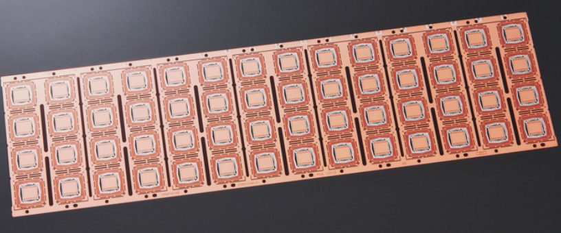
A QFN Lead Frame is an essential component in the packaging of integrated circuits (ICs), particularly in QFN (Quad Flat No-lead) packages. It serves as the physical structure that supports the IC and connects it electrically to the external circuitry of a device. Essentially, the lead frame provides the platform on which the IC is mounted, while also enabling the electrical signals to pass from the chip to the circuit board.
Structure of a QFN Lead Frame
The QFN Lead Frame is typically made from high-quality metals, with copper being the most common choice due to its excellent electrical conductivity and cost-effectiveness. In some cases, the lead frame may be alloyed with gold, silver, or other metals to enhance performance, particularly in high-frequency or high-temperature applications. These materials help to ensure the durability, heat dissipation, and overall reliability of the package.
Function of the QFN Lead Frame
The primary function of the QFN Lead Frame is twofold. First, it physically holds the IC in place, ensuring it remains securely attached within the package. Second, it acts as the conduit for electrical connections, providing a path for signals and power to flow from the IC to the device’s external circuit board. The lead frame’s design is crucial for the thermal and electrical performance of the QFN package, as it directly impacts how heat is dissipated and how well the IC communicates with the surrounding components.
Types of QFN Lead Frames
-
Traditional Lead Frames: These lead frames have larger, more visible leads that extend from the package, making them suitable for older packaging technologies like DIP (Dual In-line Package). While effective, these packages are often larger and less efficient than newer designs.
-
Micro Lead Frames: As technology advances, micro lead frames have emerged, offering a much smaller and more precise form factor. These are used in advanced packaging like QFN and other modern IC packages, where space is at a premium.
Materials Used in QFN Lead Frame Manufacturing
The choice of materials for QFN Lead Frame manufacturing can significantly impact the performance of the packaged IC. Copper is most commonly used due to its excellent thermal and electrical conductivity, but in high-end applications, gold and silver alloys are sometimes incorporated to enhance performance further, particularly when there is a need to manage heat dissipation effectively or meet specific signal integrity requirements.
The QFN Lead Frame is a fundamental element in the success of QFN packaging, offering both structural integrity and electrical performance needed for modern, high-performance electronic devices.
Understanding QFN Lead Frame Package
The QFN (Quad Flat No-lead) package is a popular surface-mount packaging solution for integrated circuits (ICs), widely used in modern electronics due to its compact size, efficiency, and performance. As the name suggests, the QFN Lead Frame plays a critical role in the design and functionality of the package, ensuring secure attachment of the IC and reliable electrical connections. The QFN package is often chosen for applications where space is limited, and high-performance, efficient heat dissipation is required.
Overview of QFN Lead Frame in QFN Packages
A QFN package is a type of leadless IC package that provides a flat, square, or rectangular form factor. Unlike traditional packages that use external leads to make electrical connections, the QFN package features metal pads underneath the package that connect directly to the PCB (printed circuit board). These pads allow for better mechanical strength and electrical performance, particularly in high-frequency and high-speed applications. Common use cases for QFN packages include mobile devices, automotive electronics, consumer electronics, and networking equipment, where compactness and performance are paramount.
Design Characteristics
The most distinctive feature of the QFN package is its leadless design. Instead of having leads extending from the sides, the connections are integrated directly underneath the package. This design eliminates the need for wire bonding in most cases, creating a flat package ideal for space-constrained applications. The QFN Lead Frame holds the chip in place, and its metal leads are used to transfer electrical signals between the IC and the PCB. The flat form factor of the package enables more efficient use of space on the PCB, which is especially beneficial for devices with limited board area or that require higher-density designs.
Key Features of QFN Packages
-
No Leads: The QFN package does not have traditional external leads like other package types (e.g., DIP or SOIC). Instead, it uses a set of metal pads beneath the package to make electrical connections. This leadless design enhances the reliability and robustness of the package by reducing the risk of physical damage or poor soldering. The QFN Lead Frame ensures a secure attachment of the chip to the PCB, with minimal interference from external leads, leading to improved mechanical stability and durability.
-
Thermal Dissipation: One of the most significant advantages of the QFN package is its ability to handle heat dissipation. With an exposed pad on the bottom of the package, the QFN package offers superior thermal performance compared to other packages that rely on external leads. The QFN Lead Frame facilitates effective heat transfer from the IC to the PCB, where thermal vias and copper pads can further assist in cooling. This makes the QFN package particularly useful in high-power applications that generate significant heat, such as power management ICs, voltage regulators, and RF (radio frequency) components.
-
Electrical Performance: The QFN package excels in electrical performance due to its leadless design and direct connections through the QFN Lead Frame. The package allows for shorter and more efficient signal paths, which reduces signal loss, improves integrity, and supports faster data rates. The proximity of the leads to the PCB also minimizes parasitic inductance and capacitance, making QFN packages ideal for high-speed and high-frequency applications, such as communications, networking, and RF devices.
The QFN (Quad Flat No-lead) package is an ideal choice for applications that require compact size, efficient thermal management, and high-performance electrical characteristics. The QFN Lead Frame is a key component of this package, ensuring reliable mechanical support and electrical connections for the IC, which is crucial for the continued advancement of modern electronic devices.
The Role of QFN Lead Frame in QFN Packages
The QFN Lead Frame plays a pivotal role in the design and functionality of QFN (Quad Flat No-lead) packages, acting as the central structure that ensures the integrity and performance of the entire package. By providing a reliable platform for mounting the integrated circuit (IC) and establishing electrical connections to the external PCB (printed circuit board), the QFN Lead Frame is integral to the success of this packaging technology, particularly in applications requiring high-density, high-performance electronics.
Integration of QFN Lead Frame in QFN Design
The QFN Lead Frame is strategically integrated into the QFN design to ensure optimal functionality and reliability. At the heart of the package, the lead frame connects the IC to the PCB through metal pads located underneath the package. These pads are soldered directly to the PCB, allowing electrical signals to travel between the IC and external components. This leadless design reduces the risk of mechanical damage compared to traditional leaded packages and improves the electrical efficiency of signal transmission.
The QFN Lead Frame is typically designed with an array of metal traces that carry electrical signals and provide mechanical support to the IC. Its precision in design and manufacturing ensures that the IC remains securely positioned while maintaining electrical connectivity. Additionally, the lead frame provides the necessary structural support during the manufacturing process, including die attachment, wire bonding, and molding, ensuring the IC remains firmly in place throughout its operational life.
Importance of QFN Lead Frame Quality for QFN Performance
The quality of the QFN Lead Frame directly affects the overall performance and durability of the QFN package. High-quality lead frames made from materials like copper, copper alloys, or other specialized metals ensure optimal electrical conductivity and mechanical strength. A poor-quality lead frame, on the other hand, can result in unreliable connections, signal degradation, or even package failure, especially in high-frequency or high-power applications.
The precision of the lead frame’s design is also crucial. Any inconsistencies in the alignment or placement of the metal pads can lead to issues with soldering or connectivity, compromising the integrity of the electrical signals. Moreover, the lead frame must be manufactured to exacting standards to ensure the robustness of the QFN package in extreme conditions such as temperature fluctuations or mechanical stress.
QFN Lead Frame’s Impact on Reliability
The QFN Lead Frame significantly impacts the reliability and longevity of the QFN package. The material chosen for the lead frame, such as copper or copper alloys, directly affects heat dissipation, thermal expansion, and mechanical stress resistance. For example, copper’s excellent thermal conductivity helps to disperse heat away from the IC, preventing overheating and ensuring stable performance over time. On the other hand, the manufacturing process must ensure that the lead frame is free from defects like warping, corrosion, or material degradation, which could undermine its performance.
The QFN Lead Frame contributes to the package’s overall durability. The mechanical strength of the lead frame ensures that the IC remains securely attached to the PCB, even in high-vibration or shock-prone environments, making QFN packages suitable for automotive and industrial applications.
QFN Lead Frame vs. Other Package Types
When compared to other packaging technologies like BGA (Ball Grid Array) or traditional leaded packages, the QFN Lead Frame offers several advantages:
-
QFN vs. BGA: While both QFN and BGA (Ball Grid Array) packages offer compact designs and excellent thermal management, the QFN Lead Frame provides a more cost-effective solution for applications where a leadless design is desired. BGA packages, with their solder balls instead of pads, can be more complex and costly to manufacture and assemble. In contrast, the QFN Lead Frame allows for easier and faster assembly with direct soldering to the PCB, reducing overall production time and cost.
-
QFN vs. Leaded Packages: Traditional leaded packages like DIP (Dual In-line Package) or SOIC (Small Outline Integrated Circuit) require external leads, making them bulkier and more difficult to integrate into modern, compact designs. The QFN Lead Frame, on the other hand, eliminates the need for these external leads, enabling a more streamlined, space-efficient design ideal for modern electronics. Additionally, the QFN package offers superior thermal dissipation and electrical performance due to the absence of leads and the presence of an exposed thermal pad.
The QFN Lead Frame is an integral component of the QFN package, providing essential structural and electrical support while also playing a significant role in the overall performance, reliability, and cost-effectiveness of the package. By ensuring secure attachment, optimal heat management, and robust electrical connections, the QFN Lead Frame continues to be a key element in the evolution of modern electronic packaging.
QFN Lead Frame vs. Other Package Types (BGA and Leaded Packages)
The QFN Lead Frame is often compared to other common packaging types, particularly BGA (Ball Grid Array) and traditional leaded packages like DIP (Dual In-line Package) or SOIC (Small Outline Integrated Circuit). Each package type has its advantages and is suited to specific applications, but the QFN Lead Frame offers distinct benefits that make it particularly well-suited for modern, high-performance electronic devices.
BGA (Ball Grid Array) vs. QFN
BGA and QFN are both widely used surface-mount packages, but they differ in several key areas, including electrical connections, size, and heat dissipation.
-
Electrical Connection:
- BGA uses small solder balls arranged in a grid pattern underneath the package, which are soldered to the PCB. These balls create a solid electrical connection that offers reliable performance, especially for high-speed signals.
- QFN, on the other hand, uses metal pads beneath the package, which are directly soldered to the PCB. This leadless design helps reduce the package’s footprint while still offering high electrical performance, as the connection is short and direct.
-
Size and Compactness:
- BGA packages can offer high pin-count configurations due to the ball grid array design, which allows for more compact routing of connections across the PCB. However, their size and complexity can make them more difficult and expensive to assemble.
- QFN packages, with their QFN Lead Frame, are generally smaller and more space-efficient. The lack of external leads results in a more compact design, making it an ideal solution for devices where minimizing board space is critical, such as in smartphones and wearables.
-
Heat Dissipation:
- Both BGA and QFN packages excel at heat dissipation, but in different ways. BGA packages typically rely on their metal balls (which act as both electrical and thermal connections) to transfer heat, and they often require additional heat sinks or vias for efficient thermal management.
- The QFN Lead Frame, however, is designed with an exposed thermal pad underneath the package, allowing for direct heat transfer to the PCB. This feature is particularly useful in high-power applications where efficient thermal management is crucial, such as in power management ICs and automotive electronics.
-
Pros and Cons of Each Package Type:
- BGA:
- Pros: High pin count, excellent electrical performance for high-speed applications, and good thermal dissipation.
- Cons: More complex and expensive to assemble, requiring precise alignment during soldering. Troubleshooting can also be challenging, as the solder balls are hidden underneath the package.
- QFN:
- Pros: More compact, cost-effective, and easier to assemble compared to BGA. The QFN Lead Frame also offers superior heat dissipation and mechanical durability.
- Cons: Limited pin count compared to BGA, which makes it less suitable for applications requiring a large number of connections.
- BGA:
Leaded Packages vs. QFN
Traditional leaded packages like DIP and SOIC were commonly used before the advent of modern, high-density packaging solutions. While they still have their place in certain applications, QFN packages have largely replaced them in modern electronic devices due to their efficiency and performance benefits.
-
DIP and SOIC Packages:
- DIP packages feature leads extending from either side of the IC, which are inserted into the PCB and soldered. These are relatively simple to assemble but take up more board space compared to QFN packages.
- SOIC (Small Outline Integrated Circuit) packages also have leads, but they are smaller and more compact than DIP packages. However, they still require more board area than QFN packages.
-
Why QFNs Are More Efficient for Modern Devices:
- QFN packages with their QFN Lead Frame allow for more efficient use of space due to the leadless design. This is particularly important for modern electronic devices that require smaller and more densely packed components, such as mobile phones, wearables, and high-performance automotive electronics.
- QFN packages also eliminate the need for wire bonding (in most cases), resulting in a simpler and more cost-effective assembly process. Additionally, the QFN Lead Frame allows for superior thermal performance, which is crucial in devices with high power requirements.
-
Comparison in Terms of Mechanical and Thermal Performance:
- Leaded Packages (DIP and SOIC):
- Mechanical Performance: Leaded packages are generally less robust than QFN packages. The external leads are more prone to physical damage, especially in high-vibration environments. In contrast, the QFN Lead Frame provides a more secure mechanical connection with fewer exposed components.
- Thermal Performance: While DIP and SOIC packages can dissipate heat, they rely on external leads and often need additional heat sinks or thermal vias. In comparison, the QFN Lead Frame has an exposed thermal pad, which allows for more efficient heat dissipation directly through the PCB, making it ideal for high-power applications.
- Leaded Packages (DIP and SOIC):
While both BGA and leaded packages have their advantages, QFN packages with their QFN Lead Frame are increasingly favored in modern electronics for their compact size, superior thermal management, and cost-effectiveness. The QFN Lead Frame ensures strong mechanical support and reliable electrical connections while enabling efficient use of space and thermal dissipation. As a result, QFN packages are the go-to choice for many modern devices, especially those requiring high performance and miniaturization.
Manufacturing Process of QFN Packages Using QFN Lead Frame
The QFN Lead Frame plays a critical role in the manufacturing process of QFN (Quad Flat No-lead) packages. As the structural foundation of the package, the QFN Lead Frame provides both mechanical support and electrical connectivity for the integrated circuit (IC) inside. There are different methods of fabricating the lead frame, and the choice of technique can impact the overall quality, cost, and precision of the final package. The two most common methods for creating lead frames are punching and sawing, each with its own set of advantages and challenges.
Punch vs. Saw Lead Frame Processes
Punch Lead Frame
The punch lead frame process involves using stamping or punching techniques to create the desired shape and pattern of the lead frame from a thin metal sheet, typically copper. This method is faster and cost-effective, making it ideal for mass production. However, the punching process can sometimes leave small burrs or rough edges on the lead frame. These burrs need to be cleaned or smoothed out in subsequent stages to ensure a clean, functional lead frame.
- Advantages:
- Faster production time, suitable for high-volume manufacturing.
- Lower cost due to its simplicity and speed.
- Challenges:
- Potential for burrs or imperfections that require additional cleaning and quality control.
- Less precise in terms of edge quality compared to the sawing method.
Sawn Lead Frame
The sawn lead frame process, on the other hand, uses a precision sawing technique to cut the lead frame from a metal sheet. This method is more precise than punching, resulting in cleaner edges and better overall quality. It is typically used for more high-end or specialized applications where precision is critical.
- Advantages:
- Higher precision and cleaner edges, reducing the need for further cleaning.
- Better control over the thickness and alignment of the lead frame.
- Challenges:
- Slower production speed, making it less suitable for high-volume manufacturing.
- Higher cost due to the need for more precise equipment and slower throughput.
Steps in QFN Package Assembly
The process of assembling a QFN package involves several steps, with the QFN Lead Frame playing an essential role in each. The QFN Lead Frame provides both structural support and the electrical paths needed to connect the IC to the PCB (printed circuit board). Below are the main steps involved in the assembly process:
Die Attachment
In the first step, the IC die is attached to the QFN Lead Frame using a strong adhesive or conductive epoxy. The lead frame serves as the platform for the die, ensuring that it remains securely in place during the rest of the assembly process. The QFN Lead Frame also helps in dissipating heat away from the die, ensuring thermal management from the very beginning.
Wire Bonding
Once the die is attached, wire bonding is performed to establish electrical connections between the IC die and the metal pads on the QFN Lead Frame. Thin gold or aluminum wires are used to connect the die’s pads to the lead frame’s electrical leads. This step is crucial for enabling communication between the IC and the external circuitry once the package is mounted onto a PCB.
Mold Encapsulation
The final step involves mold encapsulation, where the QFN Lead Frame and the bonded die are encapsulated in a protective plastic or epoxy mold. This step helps protect the IC from mechanical damage, moisture, and environmental factors. The QFN Lead Frame remains exposed at the bottom of the package, where it serves as a thermal pad for heat dissipation.
During the mold encapsulation process, the QFN Lead Frame provides support to the mold, ensuring that the die remains correctly positioned and the package’s shape is maintained. The exposed pads on the lead frame also remain available for soldering onto the PCB, which is essential for the final assembly of the device.
How the Lead Frame Provides Support Throughout the Process
Throughout the QFN package assembly, the QFN Lead Frame serves as the backbone of the entire process. It not only supports the IC die physically but also ensures that the electrical connections are made precisely during wire bonding. The frame holds the die in the correct position and ensures that the entire structure remains stable during mold encapsulation.
The QFN Lead Frame acts as a heat sink, helping to manage thermal stress and ensuring that the IC operates within safe temperature limits. Its design allows for efficient heat dissipation through the exposed thermal pad, which comes into direct contact with the PCB once the package is soldered into place. This thermal management feature is especially important in high-power applications where heat buildup could affect performance or cause damage to the IC.
The QFN Lead Frame plays a central role in the manufacturing and assembly of QFN packages. Whether using the punch or saw process, the QFN Lead Frame ensures the structural integrity, electrical performance, and thermal management of the package. From die attachment and wire bonding to mold encapsulation and final soldering, the QFN Lead Frame is essential to creating a reliable, high-performance QFN package.
The Advantages of Using a QFN Lead Frame in Packages
The QFN Lead Frame provides numerous advantages in the manufacturing and functionality of QFN (Quad Flat No-lead) packages. By incorporating a QFN Lead Frame, manufacturers can achieve cost-effective, compact designs without sacrificing performance or reliability. Below, we explore the primary benefits of using lead frames in QFN packages, focusing on cost, design, performance, and heat dissipation.
Cost-effectiveness
One of the major advantages of QFN packages that utilize the QFN Lead Frame is their cost-effectiveness compared to other packaging options. Lead frame-based QFN packages are typically less expensive to produce than BGA (Ball Grid Array) or traditional leaded packages. The QFN Lead Frame simplifies the manufacturing process because it eliminates the need for complex ball-grid arrays or external leads, reducing the cost of production and assembly.
While BGA packages offer high-performance connections, they require more intricate and expensive manufacturing steps, such as precise ball placement and reflow soldering. In contrast, QFN packages with QFN Lead Frames use a direct soldering method through the metal pads beneath the package, which is more straightforward and cost-efficient. The simplified production and lower material costs make QFN packages an ideal solution for high-volume applications where cost efficiency is key, such as consumer electronics, automotive systems, and mobile devices.
Compact Design
QFN packages, featuring the QFN Lead Frame, provide a highly compact and space-saving design. The leadless structure of QFN packages eliminates the need for external leads, allowing for a smaller footprint on the PCB. This is particularly important for modern electronic devices where maximizing available space on the circuit board is crucial. The QFN Lead Frame enables a higher density of components on the PCB, which is ideal for portable devices like smartphones, wearables, and IoT devices.
The small and flat form factor of the QFN package with its QFN Lead Frame allows for better layout flexibility, making it easier to design smaller and thinner devices. This compactness also reduces the overall device weight, making QFN packages well-suited for applications where size and weight are critical considerations, such as in aerospace, automotive, and medical devices.
Performance
The QFN Lead Frame contributes significantly to the superior electrical performance of QFN packages. The leadless design of QFN packages reduces parasitic inductance and capacitance, improving signal integrity and enabling faster data transmission. This design feature is crucial for high-speed and high-frequency applications, such as communication systems, networking equipment, and RF (radio frequency) components.
The QFN Lead Frame ensures that the electrical connections between the IC and the PCB are short and direct, minimizing signal loss and reducing interference. This is particularly beneficial in circuits that require high-frequency operations, where even small losses in signal quality can significantly impact performance. The direct connection from the IC to the QFN Lead Frame and the PCB helps maintain the integrity of high-speed signals, contributing to faster data rates and more reliable communication.
Heat Dissipation
Efficient heat dissipation is one of the most critical factors in ensuring the reliability and longevity of electronic components. The QFN Lead Frame excels in this area by providing an exposed thermal pad on the bottom of the package. This thermal pad comes into direct contact with the PCB, allowing for effective heat sinking. The QFN Lead Frame design facilitates heat transfer away from the IC and into the PCB, where thermal vias and copper pads can further assist in spreading the heat throughout the board.
The exposed thermal pad is a key advantage for QFN packages compared to other types of packages, like DIP (Dual In-line Package) or SOIC (Small Outline Integrated Circuit) packages, which may not provide the same level of heat dissipation. In high-power applications, such as power management ICs or automotive sensors, efficient heat dissipation is crucial to prevent overheating and ensure stable operation.
The QFN Lead Frame supports this thermal management by maintaining structural integrity under high thermal stress. The materials used in the QFN Lead Frame, typically copper or copper alloys, are excellent conductors of heat, further enhancing the package’s ability to handle heat. This makes QFN packages particularly suitable for applications where both high performance and thermal reliability are required, such as in high-power consumer electronics, automotive systems, and industrial control systems.
The QFN Lead Frame provides several key advantages that make QFN packages an excellent choice for modern electronic devices. They offer a cost-effective solution compared to other packaging methods like BGA, while delivering a compact design that maximizes PCB real estate. The QFN Lead Frame also contributes to better electrical performance, with improved signal integrity and faster transmission speeds. Moreover, its ability to efficiently dissipate heat ensures the stability and longevity of the package, even in high-power applications. For manufacturers and designers, the QFN Lead Frame is a vital component that enhances the overall performance, cost-efficiency, and thermal management of QFN packages, making it an ideal choice for a wide range of applications.
Applications of QFN Packages with QFN Lead Frames
The QFN Lead Frame plays a pivotal role in a wide array of applications across various industries. Its compact size, efficient heat dissipation, and excellent electrical performance make it a popular choice for many modern electronic devices. Below, we explore the key sectors where QFN packages with QFN Lead Frames are widely used, highlighting their versatility and critical role in advanced technologies.
Consumer Electronics: Smartphones, Tablets, Wearables, etc.
In the consumer electronics sector, QFN packages with QFN Lead Frames are essential components in devices that require high performance in a compact form factor. Smartphones, tablets, and wearables, for example, demand space-efficient packaging without sacrificing power or speed. The QFN Lead Frame supports the electrical and thermal needs of these devices, making it an ideal choice for the densely packed circuitry inside modern electronics.
-
Smartphones and Tablets: As mobile devices continue to shrink in size while increasing in functionality, the QFN Lead Frame enables manufacturers to integrate more components into smaller spaces. The QFN package’s small footprint, combined with its superior heat dissipation capabilities, ensures that mobile devices maintain optimal performance while remaining thin and lightweight.
-
Wearables: Devices like smartwatches and fitness trackers, which are often subject to tight design constraints, benefit from the compactness of QFN packages. The QFN Lead Frame’s space-saving design allows for a high-density component layout, which is crucial in wearables that require multiple sensors, communication chips, and power management units in a minimal package size.
Automotive Industry: ECUs, Sensors, and Power Modules
The automotive industry relies heavily on QFN packages with QFN Lead Frames for various applications, from engine control units (ECUs) to advanced sensors and power modules. As vehicles become smarter and more connected, the demand for compact, high-performance components has increased significantly.
-
ECUs (Engine Control Units): Modern vehicles use ECUs to control critical systems, such as engine management, safety features, and infotainment. QFN packages, with their QFN Lead Frames, provide the reliability and performance needed to handle the electrical and thermal demands of automotive ECUs.
-
Sensors: Automotive sensors, such as those for collision detection, temperature regulation, and tire pressure monitoring, benefit from the QFN Lead Frame design. These sensors often require robust, high-performance packaging to operate reliably in harsh environments, and the QFN Lead Frame’s thermal and electrical capabilities make it an ideal choice.
-
Power Modules: Power modules that control electric motor functions and battery management in electric vehicles (EVs) also use QFN packages. The QFN Lead Frame allows for effective thermal management, ensuring the stability of power electronics during operation, particularly in high-power applications like EV charging stations and electric drive systems.
Communications: Networking Devices, 5G Equipment
The QFN Lead Frame is also a key player in the telecommunications and networking industries, where high-speed data transmission and signal integrity are paramount. As the demand for faster communication and better connectivity grows, especially with the advent of 5G, QFN packages have become crucial in the development of cutting-edge devices.
-
Networking Devices: Routers, switches, and modems require reliable, high-performance components that can handle high-speed signals and data transmission. QFN packages with QFN Lead Frames provide the necessary electrical performance, ensuring stable signal integrity and low loss in networking hardware.
-
5G Equipment: The transition to 5G networks has increased the demand for efficient and fast data transmission. QFN packages with QFN Lead Frames are used in components like RF (radio frequency) chips, amplifiers, and antennas, where low inductance, fast data rates, and minimal signal distortion are crucial for 5G applications. The QFN Lead Frame’s ability to dissipate heat efficiently also ensures that 5G devices can operate under high power loads without overheating.
Other Industries: Medical Devices, Industrial Controls, etc.
Beyond consumer electronics, automotive, and communications, QFN packages with QFN Lead Frames are employed in a wide range of other industries, where reliability, compactness, and performance are key considerations.
-
Medical Devices: In the medical sector, where reliability and miniaturization are critical, QFN packages are used in devices such as diagnostic equipment, patient monitoring systems, and medical implants. The QFN Lead Frame provides the required structural support and electrical connections for precise, high-performance medical components. Furthermore, the QFN Lead Frame’s thermal properties ensure that medical devices function safely under a variety of environmental conditions.
-
Industrial Controls: Industrial applications, such as automation, robotics, and factory equipment, benefit from the QFN Lead Frame in components that require high-speed processing and rugged reliability. These devices often need to withstand challenging environments, including exposure to high temperatures, vibration, and electromagnetic interference. QFN packages offer a compact, robust solution for these applications, ensuring performance even under demanding industrial conditions.
The QFN Lead Frame is an essential component in a wide range of industries due to its cost-effectiveness, compact design, and superior performance. From consumer electronics to the automotive industry, communications, and medical devices, QFN packages provide reliable, high-performance solutions for modern devices that require both space efficiency and powerful functionality. As the demand for smaller, faster, and more reliable electronic devices continues to grow, the versatility of the QFN Lead Frame will remain a crucial factor in meeting these challenges across diverse sectors.
Challenges and Future of QFN Packages with QFN Lead Frames
While QFN packages with QFN Lead Frames offer numerous advantages, there are several challenges associated with their manufacturing and application. These challenges, however, also present opportunities for innovation and improvement in the future. In this section, we explore the main obstacles faced by QFN packages and the future trends that could shape their development.
Challenges
Complex Manufacturing Processes
One of the primary challenges in the production of QFN packages with QFN Lead Frames lies in the complexity of the manufacturing process. Creating the lead frame itself involves precise metal stamping or sawing, and it requires careful handling of materials to ensure consistency and reliability. The intricate design of the QFN Lead Frame, which often includes fine-pitched leads, demands advanced techniques for manufacturing and assembly. Even slight variations in lead frame dimensions or material quality can impact the overall performance and reliability of the QFN package.
As QFN packages are increasingly used for high-frequency or high-speed applications, the manufacturing process must be refined to ensure low parasitic inductance and capacitance. This requires more advanced equipment and more stringent quality control during production, which can increase costs and lead times. These complexities may present challenges for companies looking to scale up production while maintaining the necessary level of precision.
Issues Related to High-frequency Applications and Miniaturization
Another challenge faced by QFN packages with QFN Lead Frames is the performance of high-frequency signals. As devices become more miniaturized and faster, QFN packages are often required to support high-frequency applications, such as those found in 5G communications, RF modules, and advanced automotive sensors. However, as the size of the package decreases, the QFN Lead Frame must maintain its ability to handle high-speed signals without introducing interference or signal degradation. This becomes particularly difficult in QFN packages that are smaller and have more tightly packed components.
The continued trend toward miniaturization increases the difficulty of ensuring reliable heat dissipation. Smaller packages must still effectively manage heat, which can be a challenge when components are densely packed within the QFN package. As such, while QFN Lead Frames are designed to be compact, they must still provide sufficient thermal performance to ensure the longevity and stability of the device.
Future Trends
Advanced Packaging Technologies: System-in-Package (SiP) and 3D Packaging
As the demand for smaller, more powerful devices grows, the future of QFN packages with QFN Lead Frames is likely to involve the integration of advanced packaging technologies. System-in-Package (SiP) technology, for example, is an emerging trend where multiple components, such as sensors, power management ICs, and microprocessors, are integrated into a single package. This type of packaging reduces the need for multiple separate components on a circuit board and improves overall system performance while maintaining a small footprint.
3D packaging techniques, where components are stacked vertically rather than spread horizontally, could be used in conjunction with QFN Lead Frames to further reduce size and increase the number of components that can be integrated into a single device. This would enable even higher levels of miniaturization, offering significant benefits for consumer electronics, wearables, and other high-performance applications. The QFN Lead Frame, with its ability to handle complex designs and provide effective thermal management, is likely to be at the heart of these advancements.
Potential Developments in Lead Frame Material Innovations
In the future, we can expect to see innovations in the materials used for QFN Lead Frames. Currently, copper and copper alloys are the primary materials used due to their excellent conductivity and cost-effectiveness. However, as electronic devices become more advanced, there will be increasing pressure to enhance the thermal and electrical performance of the QFN Lead Frame.
Research into alternative materials, such as advanced copper alloys or even materials with better thermal conductivity and higher electrical performance, may help address the challenges of miniaturization and high-frequency applications. Additionally, incorporating new materials that can reduce manufacturing costs or improve the sustainability of QFN packages could open up new opportunities for the widespread adoption of QFN Lead Frames in diverse industries.
Integration of Multiple Components in a Single Package
Another promising future trend is the integration of multiple components into a single QFN package with a QFN Lead Frame. This trend is driven by the need for smaller, more efficient devices that can perform a wider range of functions while taking up less space. The QFN Lead Frame could be used as a platform for integrating various types of ICs, passive components, and sensors, creating highly sophisticated systems that are ready to be deployed in a variety of applications.
This could have significant implications for industries like healthcare, automotive, and IoT, where small and highly integrated systems are becoming increasingly important. For example, in medical devices, a single QFN package could integrate a microprocessor, memory, power management, and sensors, all while maintaining the compact and durable structure provided by the QFN Lead Frame. This level of integration would reduce the need for complex assembly processes and lower the overall cost of producing advanced electronic systems.
The future of QFN packages with QFN Lead Frames holds immense potential, as technological advancements continue to shape the way electronic devices are designed and manufactured. While there are challenges, particularly around complex manufacturing processes, high-frequency applications, and miniaturization, these obstacles also present opportunities for innovation. With developments in advanced packaging technologies like System-in-Package (SiP), 3D packaging, and material innovations, the QFN Lead Frame will continue to evolve to meet the demands of next-generation electronics. The continued focus on integration and miniaturization will ensure that QFN packages remain a key solution in the future of electronics across various industries.
FQAs Abut QFN Lead Frame
What is the difference between BGA and QFN?
BGA (Ball Grid Array) and QFN (Quad Flat No-lead) are both types of surface-mount packaging for integrated circuits, but they have significant differences:
- BGA (Ball Grid Array): It uses solder balls arranged in a grid pattern on the bottom of the package to make electrical connections to the PCB. BGAs are known for their ability to support high pin counts and better thermal dissipation.
- QFN (Quad Flat No-lead): This package has no leads protruding from the sides. It uses flat pads underneath the package for electrical connections, making it more compact. It offers excellent thermal performance through its exposed thermal pad.
What is the difference between QFN and leaded packages?
QFN and leaded packages differ in their design and mounting techniques:
- QFN (Quad Flat No-lead): This package has no leads on the sides, instead using flat pads for soldering to the PCB. It provides a compact design and better thermal performance through its exposed pad.
- Leaded Packages: These packages, such as DIP (Dual In-line Package) or SOIC (Small Outline Integrated Circuit), have leads that extend from the sides of the package, which are inserted into holes on the PCB. While these packages are simpler to assemble, they require more space and are less efficient in thermal dissipation compared to QFNs.
What is the difference between punch QFN and sawn QFN?
Punch QFN and sawn QFN refer to different manufacturing methods for creating QFN lead frames:
- Punch QFN: This method uses stamping or punching to create the lead frame. It’s faster and suitable for high-volume production, but the punching process may leave burrs that require additional cleaning.
- Sawn QFN: In this method, the lead frame is created by sawing. It’s typically slower but offers more precise and cleaner cuts compared to punching, which can be advantageous for smaller lead pitches and higher precision requirements.
What is meant by lead frame?
A lead frame is a metal structure used in semiconductor packaging to hold the integrated circuit (IC) and provide electrical connections between the IC and the external circuitry (like the PCB). The lead frame serves as the foundation for packaging types such as QFN and BGA. Typically made of copper or copper alloys, the lead frame consists of leads (or pads) for electrical connection, and sometimes an exposed thermal pad for heat dissipation. It is a crucial component that supports the IC throughout the manufacturing process.

