
Advantages of Plastic Dual In-line Package(PDIP) Lead Frame
The Plastic Dual In-line Package(PDIP) Lead Frame is a widely used electronic packaging solution, known for its versatility and cost-effectiveness. PDIP features two parallel rows of pins, allowing for easy insertion into printed circuit boards (PCBs), making it ideal for through-hole mounting and manual soldering. Its importance in the electronics industry lies in its reliability, durability, and ability to house various types of integrated circuits, such as microcontrollers and operational amplifiers. This article aims to provide a comprehensive analysis of the Plastic Dual In-line Package(PDIP) Lead Frame, exploring its structure, manufacturing process, and role in enhancing the performance of PDIP packages, offering insights into its continued use in consumer electronics, industrial control systems, and more.
Overview of Plastic Dual In-line Package(PDIP) Lead Frame and DIP Technology
Definition and Key Features
The Plastic Dual In-line Package(PDIP) Lead Frame is a type of Dual In-line Package (DIP), a widely used semiconductor packaging format designed for ease of assembly and reliable electrical connections. A DIP package consists of a rectangular housing with two parallel rows of pins extending from its longer sides. These pins are designed for through-hole mounting on a printed circuit board (PCB) or insertion into a socket, making DIP a preferred choice for prototyping and applications requiring easy component replacement.
Key features of DIP packages, including the Plastic Dual In-line Package(PDIP) Lead Frame, include:
- Through-hole mounting: Ensures a strong mechanical connection to the PCB.
- Ease of handling: Can be manually soldered or inserted into sockets without specialized surface-mount equipment.
- Mechanical durability: The lead frame inside provides structural integrity and maintains consistent electrical performance.
- Standardized pin spacing: Typically 2.54mm (0.1 inches), making it compatible with breadboards and conventional PCB designs.
Common Applications of DIP
The Plastic Dual In-line Package(PDIP) Lead Frame and other DIP variants have been widely used in numerous electronic applications, including:
- Microprocessors & Microcontrollers: Many early microprocessors, including Intel’s early models, were housed in DIP packages due to their robust design and easy integration. Even today, some low-power microcontrollers still utilize PDIP for educational and industrial applications.
- Memory Chips: Early RAM and ROM chips were commonly packaged in DIP, allowing for easy expansion and replacement.
- Analog & Digital Integrated Circuits (ICs): Operational amplifiers, timers (e.g., the 555 timer), logic gates, and other ICs use DIP packaging for ease of prototyping and soldering.
- Power Management ICs: Voltage regulators and power drivers are sometimes available in DIP format for applications requiring high mechanical reliability.
- Educational & DIY Projects: Due to their ease of use, DIP-packaged components are commonly used in learning environments and hobbyist electronics.
Types of DIP Packages: PDIP, CDIP, and Their Differences
There are multiple variations of DIP packages, with Plastic Dual In-line Package(PDIP) Lead Frame and Ceramic Dual In-line Package (CDIP) being the most common:
-
Plastic Dual In-line Package (PDIP) Lead Frame:
- Made of plastic molding, offering a cost-effective solution.
- The lead frame inside ensures strong electrical and mechanical performance.
- Suitable for general consumer electronics, prototyping, and industrial applications.
-
Ceramic Dual In-line Package (CDIP):
- Uses ceramic material instead of plastic, providing higher thermal stability.
- Often used in aerospace, military, and high-reliability applications where heat resistance and durability are critical.
- More expensive compared to PDIP due to its specialized material properties.
The choice between PDIP and CDIP depends on cost, durability, and application-specific requirements. While PDIP is dominant in consumer electronics and educational fields, CDIP remains essential for mission-critical applications where high reliability is needed.
Basic Characteristics of Plastic Dual In-line Package(PDIP) Lead Frame
Physical Structure: Dual-row Through-hole Design
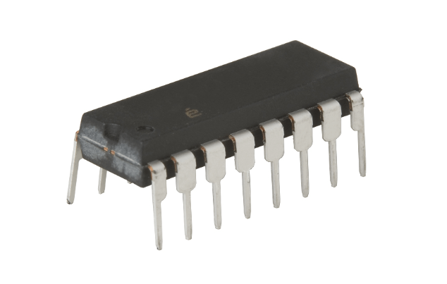
The Plastic Dual In-line Package(PDIP) Lead Frame features a rectangular body with two parallel rows of pins extending from its longer sides. These pins are designed for through-hole mounting, meaning they pass through holes in a printed circuit board (PCB) and are soldered on the opposite side. This design ensures a strong mechanical connection, making PDIP components highly reliable in environments where vibrations or movement may occur.
The package body is typically made of molded plastic, encapsulating the internal semiconductor die and lead frame, which serves as the electrical and structural foundation of the component. The dual-row layout allows for straightforward circuit board design, as the pins are spaced in a predictable and standardized manner.
Pin Configuration (Pin Spacing, Number of Pins, etc.)
The Plastic Dual In-line Package(PDIP) Lead Frame follows standardized pin configurations to ensure compatibility with PCBs and IC sockets. The most common characteristics include:
- Pin spacing: Typically 2.54mm (0.1 inches) between adjacent pins, allowing easy placement on breadboards and standard PCBs.
- Pin count: Varies from 4 to 64 pins, with common sizes including 8, 14, 16, 28, and 40 pins.
- Pin numbering: Pins are numbered counterclockwise from the notch or dot marker on the package.
- Lead shape: Leads are usually straight or slightly bent outward to facilitate insertion into PCB holes or sockets.
Encapsulation Material: Plastic vs. Ceramic (Comparison between PDIP and CDIP)
PDIP and CDIP differ mainly in their encapsulation material, impacting their durability, cost, and performance.
-
Plastic Dual In-line Package (PDIP) Lead Frame:
- Encased in plastic molding, making it lightweight and cost-effective.
- Provides sufficient protection for most consumer and industrial applications.
- Used in low-to-medium performance environments where extreme temperature tolerance is not required.
-
Ceramic Dual In-line Package (CDIP):
- Encased in a ceramic shell, offering superior thermal and mechanical stability.
- Ideal for harsh environments such as aerospace, military, and industrial automation.
- More expensive than PDIP due to its advanced material properties.
Advantages and Disadvantages
Pros of Plastic Dual In-line Package(PDIP) Lead Frame
- Cost-effective: The plastic molding and lead frame manufacturing process are economical, making PDIP widely available and affordable.
- Easy for manual soldering: Through-hole pins make PDIP ideal for hand soldering, prototyping, and DIY electronics.
- Compatible with through-hole PCBs: The Plastic Dual In-line Package(PDIP) Lead Frame is well-suited for PCBs that require secure and reliable mechanical connections.
- Reusability: PDIP chips can be easily inserted into and removed from IC sockets without damaging the component or PCB.
Cons of Plastic Dual In-line Package (PDIP) Lead Frame
- Larger package size: Compared to surface-mount technology (SMT) packages like SOIC and QFP, PDIP takes up more space on the PCB.
- Not ideal for high-density circuits: The through-hole design limits the ability to create compact, high-performance PCBs where space optimization is critical.
- Limited in high-frequency applications: Due to longer lead lengths, PDIP packages may exhibit higher parasitic inductance and resistance, affecting signal integrity in high-speed circuits.
Despite these limitations, the Plastic Dual In-line Package(PDIP) Lead Frame remains a reliable and widely used packaging solution for many applications, particularly in prototyping, educational electronics, and industrial settings where durability and ease of use are prioritized.
The Role of Lead Frame in Plastic Dual In-line Package(PDIP) Lead Frame
What is a Lead Frame?
A lead frame is a critical internal structural component of semiconductor packaging, including the Plastic Dual In-line Package(PDIP) Lead Frame. It serves as both the electrical connection medium between the integrated circuit (IC) and the external circuit board and as a mechanical support structure that holds the semiconductor die in place. The lead frame is composed of thin metal strips that extend outward as leads (pins), which are later bent to form the characteristic dual in-line configuration of PDIP.
In the Plastic Dual In-line Package(PDIP) Lead Frame, the lead frame is encapsulated in plastic molding, leaving only the external pins exposed for connection. This component plays a vital role in ensuring reliable electrical performance, efficient heat dissipation, and structural stability for the entire package.
Materials Used for Lead Frames
The choice of material for the lead frame in Plastic Dual In-line Package(PDIP) Lead Frame packaging significantly affects electrical conductivity, thermal performance, and mechanical strength. Common materials include:
- Copper Alloy: The most widely used material due to its high electrical conductivity, good thermal dissipation, and excellent mechanical strength. Copper alloy lead frames ensure low resistance connections between the IC die and PCB.
- Iron-Nickel Alloy (Alloy 42): Composed of 42% nickel and 58% iron, this material is known for its low thermal expansion coefficient, making it ideal for applications where thermal stability is critical. However, its electrical conductivity is lower than copper.
- Copper-Molybdenum (Cu-Mo) or Copper-Tungsten (Cu-W) Composites: These materials are used in high-power or high-frequency applications that require superior thermal conductivity and mechanical stability.
- Silver or Gold Plating: Often applied to lead frames to enhance solderability, corrosion resistance, and electrical performance.
Lead Frame Manufacturing Process
The lead frame in Plastic Dual In-line Package(PDIP) Lead Frame packaging undergoes multiple precision manufacturing steps to ensure high quality and performance:
- Stamping: A high-speed stamping process is used to cut and shape the lead frame from a metal sheet. This method is cost-effective for mass production.
- Etching: A chemical etching process can be used as an alternative to stamping, offering greater precision and design flexibility for fine-pitch lead frames.
- Electroplating: The lead frame is coated with a thin layer of materials such as silver, gold, tin, or palladium to enhance electrical conductivity and protect against oxidation.
- Molding Encapsulation: After the semiconductor die is bonded to the lead frame and wire bonding is completed, the entire assembly is encapsulated in plastic molding to form the final PDIP package.
Impact of Lead Frame on Thermal Dissipation, Mechanical Stability, and Electrical Performance
The Plastic Dual In-line Package(PDIP) Lead Frame directly influences the overall performance of the semiconductor package in multiple ways:
- Thermal Dissipation: The lead frame acts as a thermal conductor, transferring heat away from the semiconductor die to the PCB. Copper-based lead frames provide superior heat dissipation, preventing overheating and improving the longevity of electronic components.
- Mechanical Stability: The lead frame provides structural support to the semiconductor die, ensuring the package can withstand mechanical stress, vibrations, and thermal expansion. This is particularly important in industrial and automotive applications, where durability is essential.
- Electrical Performance: The lead frame establishes electrical connections between the IC and external circuits, minimizing resistance and ensuring efficient signal transmission. High-quality electroplating on the lead frame enhances solderability and prevents oxidation, which is crucial for maintaining long-term reliability.
The package depends on a well-designed lead frame to achieve optimal electrical conductivity, mechanical robustness, and thermal management. These characteristics make it a reliable and cost-effective choice for various electronic applications, from consumer electronics to industrial control systems.
PDIP Package Manufacturing Process: Plastic Dual In-line Package(PDIP) Lead Frame
The Plastic Dual In-line Package(PDIP) Lead Frame manufacturing process involves multiple precise steps to ensure the final package is durable, electrically reliable, and suitable for integration into various electronic applications. This process transforms a bare semiconductor die into a fully encapsulated, leaded package ready for mounting on a printed circuit board (PCB). Below are the key stages of PDIP package production.
Die Attach (Chip Bonding)
The manufacturing process of the Plastic Dual In-line Package(PDIP) Lead Frame begins with die attach, also known as chip bonding. This step involves securing the semiconductor die onto the lead frame using specialized adhesives or solder-based bonding materials.
-
Process:
- The lead frame is positioned in place, and an adhesive material (typically silver-filled epoxy or solder paste) is applied to the die pad.
- The semiconductor die is placed precisely on the adhesive material.
- The assembly is cured or heated to ensure a strong, thermally conductive bond between the die and lead frame.
-
Purpose:
- Provides mechanical stability to hold the semiconductor die in place.
- Enhances heat dissipation from the chip through the lead frame.
Wire Bonding
Once the die is securely attached, the next step is wire bonding, which creates electrical connections between the semiconductor die and the external leads of the Plastic Dual In-line Package(PDIP) Lead Frame.
-
Process:
- A fine gold or aluminum wire is attached to the bonding pads on the semiconductor die.
- Using ultrasonic, thermal compression, or thermosonic bonding techniques, the wires are connected to the corresponding lead frame terminals.
- The bonding process ensures a low-resistance electrical connection between the die and the external circuit.
-
Purpose:
- Transfers electrical signals from the semiconductor die to the lead frame, allowing integration with external circuits.
- Ensures reliable electrical performance in various operating conditions.
Molding (Encapsulation)
To protect the delicate semiconductor die and wire bonds, the Plastic Dual In-line Package(PDIP) Lead Frame undergoes molding encapsulation using thermoset plastic materials.
-
Process:
- The lead frame with the attached semiconductor die and wire bonds is placed into a mold cavity.
- A heated epoxy-based plastic compound is injected under high pressure to completely encapsulate the die and wire bonds.
- The package is then cured in an oven to harden the plastic and ensure mechanical strength.
-
Purpose:
- Provides physical protection against environmental factors such as moisture, dust, and mechanical stress.
- Improves electrical insulation and prevents short circuits.
- Enhances the package’s long-term durability in various applications.
Trim & Form Process
After molding, the Plastic Dual In-line Package(PDIP) Lead Frame is still part of a large interconnected sheet. The trim & form process separates individual packages and shapes the leads for easy PCB mounting.
-
Process:
- The excess lead frame material is trimmed to isolate each PDIP package.
- The remaining leads are bent outward at a 90-degree angle to create the familiar dual in-line configuration.
- The leads may undergo additional plating or surface treatment to enhance solderability.
-
Purpose:
- Ensures that the lead spacing and shape meet PCB mounting specifications.
- Prepares the package for final electrical testing and integration.
Testing and Quality Control
Before the Plastic Dual In-line Package(PDIP) Lead Frame is shipped for use in electronic products, each unit undergoes rigorous testing and quality control to ensure reliability.
-
Process:
- Electrical Testing: Checks for open circuits, short circuits, and correct signal transmission.
- Thermal Testing: Evaluates the package’s ability to dissipate heat effectively.
- Mechanical Testing: Assesses the durability and lead strength under stress conditions.
- Visual Inspection: Ensures there are no cracks, defects, or misalignments in the final package.
-
Purpose:
- Guarantees that each PDIP component meets industry standards and performance specifications.
- Prevents faulty packages from being used in consumer or industrial electronics.
The manufacturing process of the Dual In-line Package involves a series of precise, high-quality steps, including die attach, wire bonding, encapsulation, lead trimming, and rigorous testing. Each stage is crucial for ensuring the reliability, durability, and electrical performance of the packaged components. This structured manufacturing approach allows this packaging solution to remain widely used and trusted in the electronics industry.
Comparison of PDIP with Other Package Types: Plastic Dual In-line Package(PDIP) Lead Frame
The Plastic Dual In-line Package(PDIP) Lead Frame is one of the most commonly used packaging types for integrated circuits. However, it is important to compare it with other package types to understand its advantages, disadvantages, and best-use scenarios. Below, we compare PDIP with CDIP, SOIC, LGA, and Chip Carrier to highlight the differences in structure, performance, and application.
Plastic Dual In-line Package(PDIP) Lead Frame vs. CDIP (Ceramic Dual In-line Package)
Both Plastic Dual In-line Package(PDIP) Lead Frame and Ceramic Dual In-line Package (CDIP) share the same dual-row, through-hole mounting configuration, but they differ in materials and performance characteristics.
| Feature | PDIP (Plastic Dual In-line Package) | CDIP (Ceramic Dual In-line Package) |
|---|---|---|
| Material | Plastic encapsulation | Ceramic encapsulation |
| Durability | Less resistant to high temperatures and moisture | Highly durable, ideal for harsh environments |
| Thermal Performance | Moderate heat dissipation | Excellent thermal resistance |
| Electrical Performance | Standard signal integrity | Lower parasitic capacitance and better electrical stability |
| Cost | Cost-effective | Expensive due to high-quality materials |
| Applications | Consumer electronics, standard ICs | Aerospace, military, and high-reliability applications |
Key Takeaways:
- PDIP is more cost-effective and suitable for general applications.
- CDIP offers better thermal and electrical performance, making it ideal for mission-critical applications like aerospace and military electronics.
Plastic Dual In-line Package(PDIP) Lead Frame vs. SOIC (Small Outline Integrated Circuit)
The Plastic Dual In-line Package(PDIP) Lead Frame and Small Outline Integrated Circuit (SOIC) differ in size, pin configuration, and mounting style. While PDIP is a through-hole package, SOIC is a surface-mount package, making them suitable for different PCB designs.
| Feature | PDIP (Plastic Dual In-line Package) | SOIC (Small Outline Integrated Circuit) |
|---|---|---|
| Mounting Type | Through-hole | Surface-mount (SMT) |
| Package Size | Larger and bulkier | Smaller and compact |
| Pin Spacing | 2.54mm (standard) | 1.27mm or less (tighter spacing) |
| Ease of Soldering | Easier for manual soldering | Requires precise automated soldering |
| Applications | General-purpose ICs, DIY projects | High-density, miniaturized circuits |
Key Takeaways:
- PDIP is easier to solder manually, making it suitable for prototyping and traditional PCB designs.
- SOIC is better for high-density circuit boards due to its smaller footprint and surface-mount design.
Plastic Dual In-line Package(PDIP) Lead Frame vs. LGA (Land Grid Array)
The Plastic Dual In-line Package(PDIP) Lead Frame and Land Grid Array (LGA) serve different purposes in electronics. LGA is a high-performance package used in modern processors and advanced ICs, whereas PDIP remains a cost-effective and easy-to-use package for standard applications.
| Feature | PDIP (Plastic Dual In-line Package) | LGA (Land Grid Array) |
|---|---|---|
| Mounting Type | Through-hole | Surface-mount |
| Pin Configuration | Dual-row leads | Array of contact pads (no leads) |
| Electrical Performance | Standard performance | High-speed signal transmission |
| Thermal Performance | Moderate | Excellent, often paired with heatsinks |
| Applications | Consumer electronics, microcontrollers | High-performance CPUs, GPUs, FPGAs |
Key Takeaways:
- PDIP is ideal for general-purpose ICs, whereas LGA is preferred for high-performance computing applications.
- LGA requires specialized PCBs and soldering techniques, making it less suitable for hobbyists or prototyping.
Plastic Dual In-line Package(PDIP) Lead Frame vs. Chip Carrier (PLCC, QFP, etc.)
Chip carriers, such as Plastic Leaded Chip Carrier (PLCC) or Quad Flat Package (QFP), are compact alternatives to Plastic Dual In-line Package(PDIP) Lead Frame with more pins and a smaller footprint.
| Feature | PDIP (Plastic Dual In-line Package) | Chip Carrier (PLCC, QFP, etc.) |
|---|---|---|
| Mounting Type | Through-hole | Surface-mount or socketed |
| Package Size | Larger | Smaller, more compact |
| Pin Count | Limited due to dual-row design | Can accommodate more pins |
| Flexibility | Good for prototyping | Better for high-density circuits |
| Applications | Standard ICs, microcontrollers | Advanced microprocessors, memory chips |
Key Takeaways:
- PDIP is simpler and easier to work with, making it an excellent choice for beginners and traditional PCB designs.
- Chip carriers provide higher pin density, making them better suited for compact and high-performance circuits.
The Plastic Dual In-line Package(PDIP) Lead Frame remains a widely used IC packaging type, offering cost-effectiveness, ease of use, and reliability. However, its limitations in size, pin density, and thermal performance make alternative packages like SOIC, LGA, and chip carriers more suitable for advanced applications. Understanding the differences between these packaging types allows engineers to select the most appropriate package based on design requirements, performance needs, and manufacturing constraints.
Applications of PDIP in Modern Electronics: Plastic Dual In-line Package(PDIP) Lead Frame
The Dual In-line Package (DIP) continues to play a crucial role in modern electronics despite the emergence of more compact surface-mount technologies. Due to its durability, ease of use, and cost-effectiveness, it remains widely used in various applications, from consumer electronics to industrial control systems and educational projects. This section explores the key areas where DIP components are still widely utilized.
Consumer Electronics
Many consumer electronics still incorporate Plastic Dual In-line Package(PDIP) Lead Frame components, particularly in microcontrollers, operational amplifiers, and other essential integrated circuits.
-
Microcontrollers:
- Many entry-level microcontrollers (such as the ATmega328 used in Arduino boards) are available in PDIP packaging, making them easy to prototype and integrate into consumer devices.
- Used in home automation, smart appliances, and embedded systems that require reliable and straightforward microcontroller solutions.
-
Operational Amplifiers:
- Widely used in audio processing, signal amplification, and sensor circuits.
- PDIP packaging allows these chips to be easily mounted on through-hole PCBs, ensuring a secure connection in consumer devices like audio mixers, speakers, and voltage regulators.
-
Memory and Logic ICs:
- Some older EPROMs, SRAMs, and logic gates are still available in PDIP format, particularly in legacy systems and repair markets.
- Ensures backward compatibility with existing electronic designs.
Industrial Control Systems
Industrial environments demand reliable, robust, and easily maintainable components, making the Plastic Dual In-line Package(PDIP) Lead Frame an ideal choice for industrial control circuits.
-
Driver Chips:
- Many motor drivers and power transistors are packaged in PDIP format, making them easy to swap or replace in industrial machinery.
- Examples include stepper motor drivers, relay control circuits, and automation controllers.
-
Power Management ICs:
- Voltage regulators, switching controllers, and power monitoring chips are often available in PDIP packages, ensuring ease of maintenance and repair in industrial settings.
- Used in factory automation, power supply units, and process control systems where reliable power distribution is critical.
-
Communication and Interface ICs:
- Some legacy communication ICs, such as RS-232/RS-485 transceivers, still use PDIP packaging, providing reliable data transmission in older industrial automation systems.
- Ensures compatibility with existing industrial protocols without the need for PCB redesigns.
Educational & DIY Electronics
One of the most significant advantages of this package is its breadboard-friendly design, making it a preferred choice for students, hobbyists, and DIY electronics enthusiasts.
-
Prototyping & Learning:
- The large pin spacing (2.54mm) allows PDIP components to be easily inserted into breadboards and perfboards without requiring soldering.
- Enables quick circuit assembly for beginners learning electronics.
-
Arduino and DIY Projects:
- Many popular microcontrollers, logic ICs, and analog chips are still available in PDIP format, allowing makers to develop custom circuits for robotics, IoT devices, and home automation projects.
- Examples include ATmega328 for Arduino, 555 timer ICs for pulse generation, and LM358 op-amps for signal processing.
-
Retro Computing & Repair:
- Vintage computers and gaming consoles often use PDIP-packaged memory chips and processors, making them essential for restoration and repairs.
- Provides an easy way to replace faulty chips without requiring advanced soldering techniques.
The Plastic Dual In-line Package(PDIP) Lead Frame remains relevant in modern electronics due to its ease of use, durability, and compatibility with through-hole PCB designs. From consumer devices and industrial automation to education and prototyping, PDIP continues to serve a crucial role in electronics development and maintenance. While surface-mount technology has become dominant, PDIP packages remain essential for applications where ease of handling, repairability, and prototyping flexibility are priorities.
Future Trends of PDIP: Plastic Dual In-line Package(PDIP) Lead Frame
As the electronics industry continues to evolve toward miniaturization, high-density PCB designs, and advanced surface-mount technologies (SMT), the role of this package type is being redefined. While it is no longer the dominant IC package, it remains relevant in low-cost applications, prototyping, and repair markets. This section explores the future outlook for this package, including its role in modern electronics, ongoing applications, and potential improvements.
The Role of DIP Packaging in an Evolving PCB Landscape
The electronics industry has shifted toward compact, high-performance components, favoring SMT packages such as SOIC, QFP, and BGA over traditional through-hole PDIP designs. However, PDIP packaging still plays a vital role in specific sectors where ease of use, reliability, and cost-effectiveness are crucial:
- Prototyping and Testing: PDIP remains a preferred choice for prototyping due to its breadboard compatibility and ease of manual soldering.
- Retro Computing and Repairs: Many legacy systems, including vintage computers and industrial controllers, continue to rely on PDIP-packaged ICs for maintenance and upgrades.
- Niche and Specialized Applications: Some low-power microcontrollers, analog circuits, and power management ICs still use PDIP packaging in hobbyist markets, small-scale manufacturing, and educational kits.
Despite the dominance of high-density PCBs, the dual in-line package continues to serve an important function in low-volume and easily serviceable electronic designs.
DIP’s Ongoing Relevance in Low-Cost and Low-Power Applications
Although miniaturization is a primary trend in electronics, PDIP packaging remains viable in low-cost, low-power applications where manufacturing simplicity and easy maintenance outweigh the need for extreme compactness.
-
Low-Cost Embedded Systems:
- Many budget-friendly microcontrollers and logic ICs (such as the PIC and AVR series) still utilize PDIP packaging.
- These are widely used in hobby projects, low-end IoT devices, and basic automation systems.
-
Analog and Power Electronics:
- Operational amplifiers (Op-Amps), voltage regulators, and power drivers continue to be produced in PDIP format for cost-sensitive applications.
- Through-hole components offer better mechanical stability in harsh environments compared to fragile SMT counterparts.
-
Educational and DIY Projects:
- PDIP ICs are beginner-friendly, allowing students and electronics enthusiasts to experiment with circuits without needing advanced soldering skills.
- Arduino, Raspberry Pi accessories, and STEM learning kits continue to incorporate PDIP-packaged ICs for accessibility.
PDIP’s ease of handling, affordability, and reliability ensure its continued use in entry-level electronics, power control systems, and legacy product support.
Potential Improvements in PDIP Technology
While Plastic Dual In-line Package(PDIP) Lead Frame technology has remained largely unchanged for decades, potential improvements could extend its relevance in modern electronics. Some of the key advancements that could enhance PDIP packaging include:
-
New Materials for Encapsulation:
- The development of thermally conductive plastics could improve heat dissipation, allowing PDIP ICs to operate more efficiently in power-intensive applications.
- Stronger, more durable plastic formulations could increase moisture resistance and enhance long-term reliability.
-
Pin Layout Optimizations:
- Traditional PDIP packages have fixed 2.54mm pin spacing, limiting the number of pins in a compact design.
- Reducing pin pitch while maintaining through-hole compatibility could allow for higher-density circuits while preserving ease of soldering.
-
Hybrid DIP-SMT Designs:
- Combining PDIP packages with SMT solder pads could enable dual-mounting options, offering greater flexibility for PCB design.
- This could allow seamless integration of PDIP chips into modern PCB layouts without sacrificing through-hole benefits.
Despite the increasing prevalence of surface-mount packaging, the Plastic Dual In-line Package(PDIP) Lead Frame remains an essential part of the electronics industry. Its ease of use, cost-effectiveness, and reliability continue to make it a viable choice for prototyping, educational electronics, low-power applications, and industrial control systems.
While PDIP packaging may not be the standard for cutting-edge electronics, improvements in materials, thermal management, and pin configuration could extend its usability for specific applications. As the demand for DIY electronics, repairability, and prototyping solutions persists, this packaging will continue to play a crucial role in the evolving electronics landscape.
FQAs Abut Plastic Dual In-line Package(PDIP) Lead Frame
What is the function of a Dual In-line Package (DIP)?
A Dual In-line Package (DIP) is an electronic component package that features two parallel rows of pins that are inserted into holes in a printed circuit board (PCB) for electrical connection. The main function of a DIP is to house and protect the integrated circuit (IC) while providing a stable and reliable electrical connection to the PCB. It allows for easy manual soldering and is commonly used in prototyping and through-hole PCB designs.
What is the difference between PDIP and CDIP?
PDIP (Plastic Dual In-line Package) and CDIP (Ceramic Dual In-line Package) are both types of DIP packages, but they differ in their encapsulation material:
- PDIP uses plastic as the encapsulation material, which is cost-effective, lightweight, and easier to manufacture. It is commonly used in mass-produced, low-cost applications.
- CDIP uses ceramic as the encapsulation material, which provides better thermal conductivity and mechanical strength. CDIP packages are typically used in applications that require higher performance, such as high-temperature environments or military-grade equipment.
What is the difference between DIP and SOP?
The primary difference between DIP (Dual In-line Package) and SOP (Small Outline Package) is the packaging and mounting style:
- DIP is a through-hole package, where the pins are inserted into holes on the PCB and soldered on the opposite side. It is larger and more suitable for manual soldering.
- SOP is a surface-mount package with pins that are soldered directly onto the surface of the PCB. It is smaller, more compact, and suited for automated manufacturing and high-density circuits.
What is a DIP chip?
A DIP chip refers to an integrated circuit (IC) that is packaged in a Dual In-line Package (DIP) format. It consists of a semiconductor chip encapsulated in a plastic or ceramic casing with two rows of pins extending from either side. These pins are used to connect the chip to a circuit board. DIP chips are commonly used in early electronics and are easily mounted on through-hole PCBs for applications like microprocessors, memory chips, and other ICs in consumer electronics, automotive, and industrial devices.

