Customized Multi-Material Package Substrates – ALCANTA
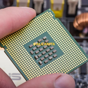
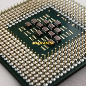
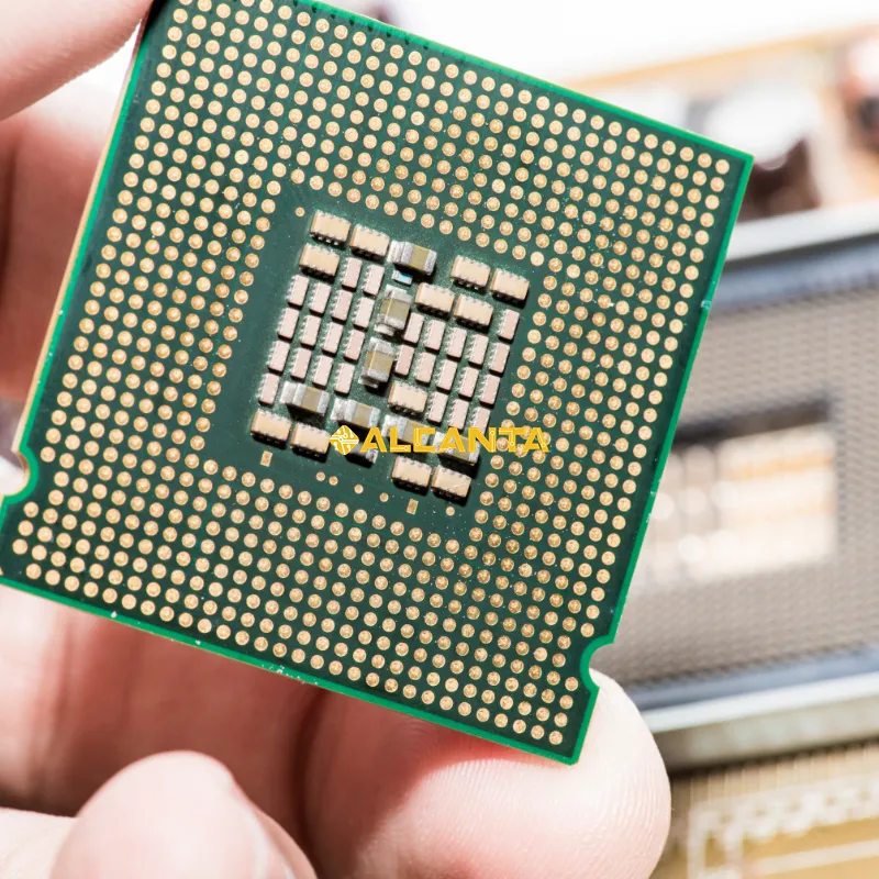
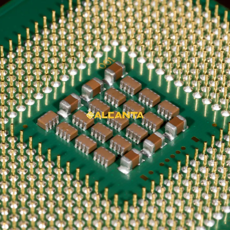
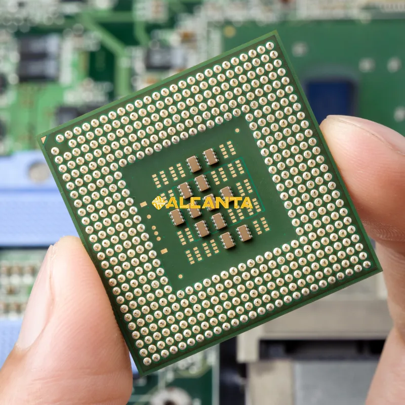
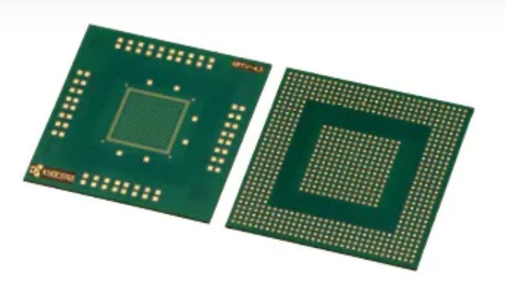
A package substrate is a critical component in semiconductor packaging, acting as the base that supports and connects integrated circuits (ICs) to the external environment. It serves multiple essential functions: providing mechanical support for the IC, ensuring electrical connectivity between the IC and external components, and aiding in thermal dissipation to prevent overheating. Package substrates are designed with multiple layers, including a core layer for structural integrity, inner layers for signal routing, and outer layers for external connections. Advanced manufacturing techniques like photolithography, lamination, and via filling ensure the substrate’s performance, particularly for high-density, high-speed, and power-intensive applications in modern electronics.
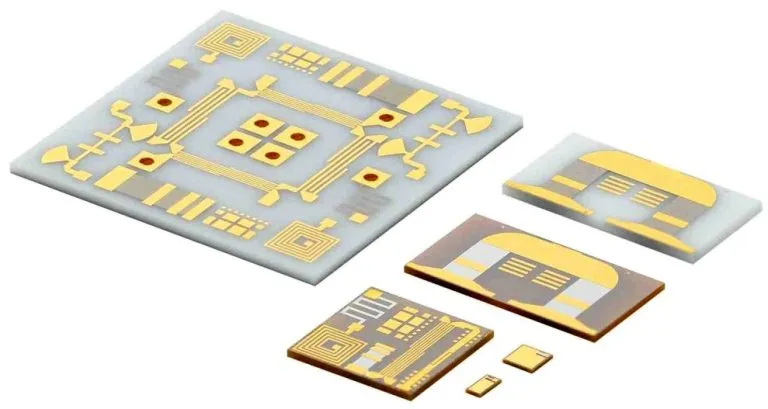
ALCANTA Offers Substrates in the Following Materials:
What is Package Substrate?
A package substrate is a key structural component in semiconductor packaging, which acts as the interface between the integrated circuit (IC) and the external electronic systems it needs to communicate with. In simple terms, it’s the base upon which an IC is mounted, connecting it to other components and ensuring that signals can flow seamlessly between the chip and the outside world.
The substrate is often made of specialized materials that fulfill several critical functions, including providing electrical interconnections, mechanical support, and heat dissipation for the IC. It is designed to support and protect the fragile semiconductor die, while also ensuring that the IC can effectively transmit signals to other parts of the electronic device. Without the package substrate, it would be nearly impossible to integrate ICs into larger systems.
Here are the main functions that a package substrate serves in semiconductor packaging:
- Electrical Interfacing:
The package substrate provides a pathway for electrical signals to flow between the IC and the rest of the device or system. This is achieved through a series of metal traces, vias, and pads embedded in or applied to the surface of the substrate. These electrical connections allow the IC to communicate with external components such as sensors, processors, and memory chips, enabling complex operations in electronic systems. - Mechanical Support:
One of the primary roles of the package substrate is to provide physical stability for the IC. Integrated circuits themselves are typically fragile, and without a secure mounting platform, the IC could be damaged during assembly or from mechanical stresses during use. The package substrate holds the IC in place and protects it from external forces. It also enables the secure attachment of the IC to the larger printed circuit board (PCB) or system. - Thermal Management:
ICs generate heat during operation, and efficient heat dissipation is crucial for maintaining their performance and preventing overheating. The package substrate helps in this thermal management by distributing the heat away from the IC. It often includes materials with high thermal conductivity, such as copper or ceramics, to ensure that heat can be transferred from the IC to the external environment. In some advanced package designs, the substrate may also include thermal vias or heat spreaders to further improve heat dissipation. - Signal Integrity and High-Speed Performance:
As electronic systems become more complex and high-speed, maintaining signal integrity has become increasingly important. The design of the package substrate directly impacts the quality of the electrical signals passing through it. For high-speed applications, such as in processors or communications chips, the substrate must be carefully engineered to reduce signal degradation, cross-talk, and electromagnetic interference (EMI). The choice of material, layout, and the number of layers in the substrate can all influence signal fidelity. - Providing a Platform for Assembly and Bumping:
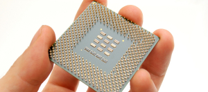
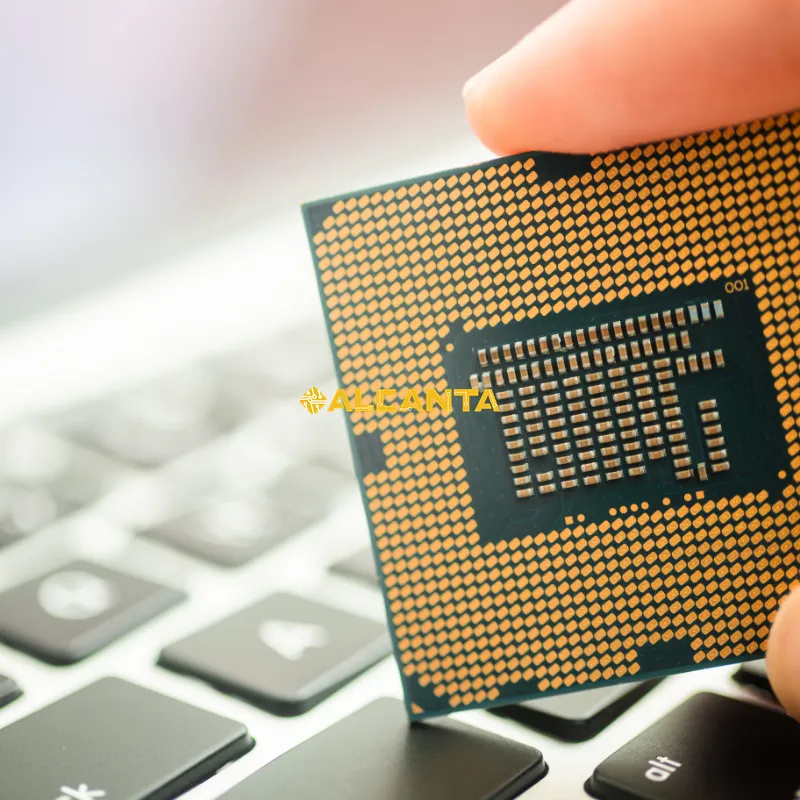
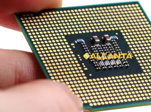
The package substrate also plays a role in the assembly process. It provides a stable platform for attaching the IC to the substrate itself, typically using solder bumps or balls in the case of ball grid array (BGA) packages. These bumps or balls allow the IC to be electrically and mechanically connected to the external circuit board. The substrate’s surface can also be designed to facilitate these interconnections, ensuring that the IC is firmly and reliably connected to the larger system.
Function of a Package Substrate
A Package Substrate is a critical carrier in semiconductor packaging, responsible for electrical interconnection, heat dissipation, and mechanical support of the chip. Based on material and structure, package substrates can be mainly categorized into the following types:
1. Organic Substrates
Materials & Structure: BT (Bismaleimide Triazine), FR-4 (Epoxy Glass), Ajinomoto Build-up Film (ABF); multi-layer composite resin structure; high-density circuits formed via copper foil lamination and photolithography.
Manufacturing: Multi-layer lamination → laser-drilled microvias → copper electroplating → photolithography → surface treatment.
Technical: Line/space 5–35 µm; relatively high CTE, must match chip material; moderate electrical performance.
Applications: FC-BGA, PBGA, CSP.
Advantages/Limitations: Low cost, mature process, high-density capability; signal loss can be significant at high frequencies.
2. Inorganic Substrates
Materials & Structure: Ceramics (Al₂O₃, AlN), glass, glass composites; multi-layer stacking after sintering, laser drilling, and metallization.
Technical: Low CTE; excellent for GHz-range devices; high reliability and thermal shock resistance.
Applications: High-frequency RF modules, 5G chips, GPUs, AI accelerators.
Advantages/Limitations: Excellent signal integrity and stable heat dissipation; high cost and complex processing.
3. Metal Core Substrates
Materials & Structure: Aluminum or copper base; insulation layer of epoxy or ceramic thin film; circuit patterning and copper electroplating.
Technical: High thermal conductivity, good heat management, high mechanical strength; limited high-frequency performance.
Applications: LED packages, power modules, power semiconductor devices.
Advantages/Limitations: Improves heat dissipation; suitable for high-power applications; not ideal for high-frequency circuits.
4. Hybrid / Composite Substrates
Materials & Structure: Combines organic, ceramic, and metal advantages; multi-layer composite for high-density interconnects and heat dissipation; precise stacking and microvia alignment required.
Technical: Strong high-density routing; good thermal performance with signal integrity; customizable structure.
Applications: AI accelerators (HPC), high-end GPUs, multi-chip packages (SiP).
Advantages/Limitations: Balances heat dissipation and high-speed signals; complex and costly; multi-layer design requires strict process control.
Selecting the right package substrate requires careful consideration of several technical factors. First, material properties are crucial: organic substrates like ABF or BT offer good manufacturability for high-density BGA packages, while inorganic materials like glass provide superior dimensional stability and low signal loss for high-frequency applications. Electrical performance, including dielectric constant, impedance control, and layer count, should match the device requirements. Thermal and mechanical characteristics, such as CTE compatibility and thermal conductivity, ensure reliability under thermal cycling and high-power operation. Manufacturing constraints and assembly compatibility, such as microvia capability and warpage behavior, must also be considered to achieve both performance and yield. ALCANTA provides a wide range of substrates across organic, inorganic, and hybrid materials, allowing engineers to select the optimal substrate for each specific application.
Main Structure and Production Technologies of Package Substrate
A package substrate is a multi-layered, sophisticated component designed to support the complex functions of modern semiconductor devices. It not only provides the physical foundation for the IC but also ensures efficient electrical, thermal, and mechanical performance. To achieve this, package substrates are engineered with specific layers and materials to meet the rigorous demands of high-performance electronics. The production of package substrates also involves advanced technologies to build up these layers, create interconnections, and ensure reliability.
Below, we delve into the main structural components of a package substrate and the key production technologies used in its manufacturing.
Structure of a Package Substrate
Package substrates are typically composed of several layers, each serving a specific function related to the packaging’s electrical, mechanical, and thermal properties. These layers are carefully designed and manufactured to ensure that the substrate can support the integrated circuit (IC) and meet its performance requirements. The general structure of a package substrate includes the following layers:
Core Layer
The core layer serves as the foundation of the package substrate. It provides mechanical strength and supports the overall structure of the substrate, maintaining its shape and stability during the manufacturing process and throughout the lifecycle of the IC package.
- Materials: The core layer is typically made from fiberglass-reinforced resin (commonly epoxy resin or polyimide) or ceramic materials (such as alumina or aluminum nitride) for applications requiring superior thermal performance. In some cases, metal cores (such as copper) are used to improve heat dissipation, especially for power devices.
- Function: The core layer serves as a structural base for the rest of the package. It must provide mechanical integrity to hold the IC securely in place and withstand the stresses from heat cycles, physical shock, and other environmental factors.
- Thickness: The core layer typically has a moderate thickness to ensure strength, with the thickness depending on the requirements of the IC and the application. For high-density interconnect (HDI) substrates, the core may be thinner to maximize space for the finer interconnects and layers.
Inner Layer
The inner layer contains the circuits and signal pathways that connect the IC’s pins or pads to the external world. This layer is crucial for routing electrical signals between the IC and the external circuitry.
- Materials: The inner layer is usually composed of conductive materials such as copper or gold. Copper is the most commonly used material due to its excellent electrical conductivity, though other materials like gold or silver may be used in specific applications requiring enhanced signal integrity.
- Function: This layer houses the signal traces, vias, and pads that enable communication between the IC and the external devices. The signal routing and interconnects in this layer must be designed to minimize signal loss, cross-talk, and other electrical interference, particularly for high-speed or high-frequency applications.
- Design Considerations: The inner layer often features fine-pitch traces (for fine-line routing) and via structures that provide vertical interconnections between layers. The quality and precision of the signal pathways in the inner layer directly impact the substrate’s performance, especially for high-frequency ICs.
Outer Layer
The outer layer is the topmost layer of the package substrate, where the solder bumps or balls are placed to establish the connection between the IC and the external system.
- Materials: This layer typically uses solder (commonly lead-free solder, such as tin-silver-copper) to create the solder balls in ball grid array (BGA) packages or solder pads in flip-chip packages. The solder balls or pads provide the electrical interface for connecting the IC to external pins, leads, or directly to a PCB.
- Function: The outer layer is where the external electrical connection is made, ensuring that the IC can communicate with the broader system. It also plays a role in distributing heat away from the IC during operation.
- Design Considerations: The placement of solder balls or pads is critical for creating reliable connections, ensuring low resistance and consistent alignment with the IC and the PCB. In BGA packages, the solder balls are arranged in a grid pattern to support high-density connections. For flip-chip packages, the solder pads facilitate the attachment of the IC directly to the substrate.
Underfill and Encapsulation
The underfill and encapsulation are additional materials applied to the package substrate after assembly to enhance reliability and protect the IC from environmental stresses.
- Underfill: This is a specialized epoxy resin or polymer material used to fill the gap between the IC and the substrate in flip-chip packages. Underfill helps to distribute thermal stress evenly, increase mechanical strength, and improve the long-term reliability of the package by preventing thermal fatigue and cracking.
- Encapsulation: After the substrate and IC are assembled, the package is often coated with a protective encapsulation (often mold compound or plastic resin) to protect the IC from moisture, dust, and mechanical shock. Encapsulation also helps with heat dissipation, although thermal management is primarily handled by the substrate and external heatsinks.
Production Technologies for Package Substrate
The manufacturing process of a package substrate involves several intricate and advanced technologies to build its multi-layered structure, create conductive pathways, and ensure that the final product meets high-performance requirements. Below are the key production technologies used in the fabrication of package substrates:
Photolithography
Photolithography is used to pattern the inner layers of the substrate, allowing for the creation of precise electrical paths (traces), vias, and other structures.
- Process: A photoresist material is applied to the surface of the substrate. Light is then passed through a photomask to selectively expose the photoresist, which is subsequently developed to leave behind a pattern of exposed or unexposed material. This pattern is used to guide the creation of conductive traces.
- Purpose: Photolithography enables the formation of intricate patterns on the substrate, including fine-pitch traces and vias needed for high-density interconnects. It is a critical process for ensuring that the substrate can handle complex signal routing and precise connections.
Laminating
Laminating involves bonding different layers of materials together to form a multi-layered substrate. This process is essential for creating the core and inner layers of the package substrate.
- Process: Multiple layers of material (often including the core material and conductive copper foil) are stacked together, and then a heat and pressure process is used to bond the layers into a solid, multi-layered structure.
- Purpose: The lamination process ensures that the different layers of the substrate adhere together and form a cohesive structure capable of supporting complex interconnections and providing mechanical stability.
Plating and Etching
Plating and etching are used to create conductive traces and vias on the surface of the substrate.
- Plating: A thin layer of metal, usually copper, is plated onto the substrate’s surface using an electroplating process. This copper layer forms the conductive pathways for electrical signals.
- Etching: The plated copper is then selectively removed (etched) using chemical processes to leave behind the desired traces and circuit patterns.
- Purpose: These processes create the metal traces and via holes that connect the various layers of the substrate, enabling electrical conductivity between different parts of the package.
Via Filling
Via filling is a process used to fill the small holes (vias) that pass through the substrate to establish electrical connectivity between different layers of the substrate.
- Process: The vias are typically filled with copper or other conductive materials, and the process may involve plating or injection molding techniques to ensure the vias are completely filled and free of voids.
- Purpose: Via filling is essential for maintaining electrical continuity between the layer
CONTACT US
Get Precise Technical Solutions!
FAQs About Package Substrate
What is a substrate in packaging?
In packaging, a substrate refers to the material or base layer upon which semiconductor chips or electronic components are mounted and interconnected. It provides structural support, electrical connectivity, and thermal management for the components within the package.
What is the difference between substrate and package?
The substrate is the underlying material or base layer where semiconductor chips are mounted, providing support and connectivity. In contrast, the package refers to the overall enclosure or housing that protects the semiconductor chip and provides external electrical connections, often including features like leads or pins for interfacing with other devices or systems.
What is a semiconductor package substrate?
A semiconductor package substrate is a specialized substrate designed specifically for mounting and interconnecting semiconductor chips within a semiconductor package. It is optimized for electrical performance, thermal dissipation, and reliability, playing a crucial role in ensuring the functionality and longevity of integrated circuits.
What is the substrate in electronic packaging?
In electronic packaging, the substrate refers to the material or base layer used for mounting and interconnecting semiconductor chips or electronic components within a package. It provides a stable platform for chip attachment, facilitates electrical connections between components, and assists in managing heat dissipation.
How does a substrate impact electronic packaging?
The substrate plays a vital role in electronic packaging by providing structural support, electrical connectivity, and thermal management for semiconductor chips or electronic components. It directly influences the performance, reliability, and miniaturization of electronic devices by facilitating efficient signal transmission, heat dissipation, and mechanical stability within the package.
What are the key considerations in selecting a substrate for electronic packaging?
When selecting a substrate for electronic packaging, key considerations include electrical properties (such as impedance and signal integrity), thermal conductivity, mechanical strength, reliability, compatibility with assembly processes, and cost-effectiveness. The substrate material and design should be carefully chosen to meet the specific requirements of the application and optimize the performance and reliability of the electronic device.
What are the primary functions of Package Substrate in electronic devices?
Package Substrate provides structural support, electrical connectivity, and thermal management for semiconductor chips within electronic packages. It facilitates efficient signal transmission, heat dissipation, and mechanical stability, ensuring optimal performance and reliability of electronic devices.
How does Package Substrate contribute to miniaturization in electronics?
Package Substrate enables miniaturization by offering compact designs with high-density interconnects, allowing for the integration of more semiconductor components within a smaller footprint. Its advanced materials and manufacturing processes optimize space utilization while maintaining performance and reliability, driving the development of sleeker and more portable electronic devices.
What are the advantages of using Package Substrate over traditional packaging methods?
Package Substrate offers several advantages, including higher packaging densities, improved thermal management, enhanced signal integrity, and greater reliability compared to traditional packaging methods. Its advanced design and materials optimize performance and efficiency, making it an ideal choice for high-performance electronic devices in various applications.
How does Package Substrate impact the overall cost of electronic products?
While Package Substrate may initially incur higher manufacturing costs due to advanced materials and processes, its benefits in terms of performance, reliability, and miniaturization can lead to cost savings in the long run. By enhancing product quality, reducing failure rates, and enabling the development of innovative features, Package Substrate contributes to overall cost-effectiveness and competitiveness in the electronics market.

