
The Advantages of Multi-Chip Leadframe Packaging in Electronics
Semiconductor packaging is essential for protecting and interconnecting devices, ensuring reliability and performance. As electronic systems grow more complex, multi-chip packaging has become a key solution, integrating multiple chips into a single package to reduce footprint, enhance electrical performance, and improve thermal management. Among various approaches, leadframe-based designs offer a cost-effective and efficient alternative to substrate-based solutions. The leadframe provides mechanical support and electrical connections while facilitating signal transmission and heat dissipation. This makes it particularly valuable in high-performance and miniaturized electronics. One advanced packaging method leveraging these benefits is Multi-Chip Leadframe, which simplifies manufacturing while maintaining high functionality. As demand for compact, high-performance semiconductor solutions continues to rise, this technology remains a crucial driver of innovation in the industry.
What is a Multi-Chip Leadframe Package?
A Multi-Chip Leadframe package is a semiconductor packaging technology that integrates multiple chips within a single leadframe-based structure. Unlike traditional single-chip packages, this approach enables multiple semiconductor dies to be placed on a shared leadframe, interconnected through wire bonding or other connection methods. This design enhances electrical performance, improves heat dissipation, and reduces overall package size while maintaining cost efficiency.
Compared to other multi-chip packaging technologies, such as System-in-Package (SiP) and Multi-Chip Module (MCM), Multi-Chip Leadframe offers a simpler and more cost-effective solution. SiP integrates multiple functional components, including memory, processors, and passive elements, using advanced substrate-based interconnections, making it highly versatile but often more expensive. MCM, on the other hand, assembles multiple dies onto a common substrate, improving integration but requiring complex fabrication processes. In contrast, Multi-Chip Leadframe packaging leverages a leadframe structure, which simplifies manufacturing, reduces costs, and provides efficient thermal management, making it ideal for high-volume and cost-sensitive applications.
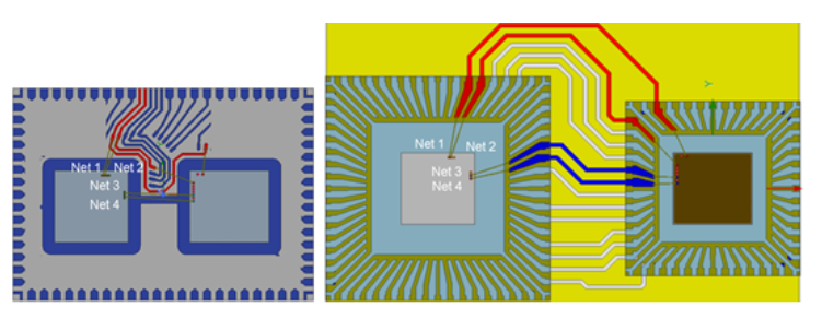
Composition and Function of Multi-Chip Leadframe
A Multi-Chip Leadframe package relies on a carefully designed leadframe structure to provide mechanical support, electrical connectivity, and thermal management for multiple semiconductor chips. The leadframe consists of a metal framework that forms the foundation of the package, featuring die pads to hold the semiconductor chips and lead fingers to establish electrical connections. These leads extend outward, enabling integration with external circuits through wire bonding or other interconnection methods.
Material selection is a critical factor influencing the performance of a Multi-Chip Leadframe package. Common materials include copper and copper alloys, which offer excellent electrical conductivity and thermal dissipation. In some cases, silver or nickel plating is applied to enhance corrosion resistance and solderability. The choice of material directly impacts the package’s reliability, electrical efficiency, and ability to dissipate heat effectively.
In addition to providing structural support, the leadframe plays a vital role in electrical connectivity and thermal management. It ensures low-resistance signal transmission between the chips and external components, minimizing power loss and enhancing performance. Moreover, the metal leadframe acts as a heat spreader, efficiently transferring heat away from the chips to prevent overheating. This thermal advantage makes Multi-Chip Leadframe packaging an ideal choice for applications requiring high power efficiency and reliability.
Design Considerations for Multi-Chip Leadframe Packages
When developing a Multi-Chip Leadframe package, several critical design factors must be carefully addressed to ensure optimal performance, reliability, and manufacturability. These considerations include chip layout and interconnection strategies, heat dissipation and thermal management, as well as electromagnetic interference (EMI) and signal integrity.
Chip Layout and Interconnection Strategies
The arrangement of multiple chips within a Multi-Chip Leadframe package significantly impacts electrical performance and thermal efficiency. An optimized layout minimizes interconnection lengths, reducing signal delay and power loss. Wire bonding remains the most commonly used interconnection method, offering a cost-effective and reliable solution for linking the chips to the leadframe. However, advanced techniques such as flip-chip bonding or stacked die configurations may be used to further enhance integration and performance. Proper isolation between different chips is also crucial to prevent electrical interference and cross-talk, ensuring stable operation.
Heat Dissipation and Thermal Management
Thermal performance is a key concern in Multi-Chip Leadframe designs, as multiple chips generate considerable heat within a confined package. The metal leadframe itself serves as an efficient heat spreader, helping to dissipate thermal energy away from the chips. To enhance heat dissipation, designers may incorporate heat slugs, thermal vias, or external heat sinks. Additionally, materials with high thermal conductivity, such as copper leadframes with silver plating, can further improve thermal performance. Effective thermal management prevents overheating, which is essential for maintaining long-term reliability and preventing performance degradation.
Electromagnetic Interference (EMI) and Signal Integrity
In high-speed and high-frequency applications, EMI and signal integrity become major design challenges for Multi-Chip Leadframe packages. Poor signal routing or improper grounding can lead to unwanted noise, affecting device performance. To mitigate EMI issues, careful shielding techniques, optimized grounding strategies, and well-planned signal paths must be implemented. Additionally, using low-inductance bonding wires and minimizing loop areas in the leadframe design help improve signal integrity. By addressing these concerns, Multi-Chip Leadframe packages can achieve stable and high-speed data transmission, making them suitable for advanced electronic applications.
By considering these key design factors, Multi-Chip Leadframe packaging can deliver enhanced electrical performance, efficient heat dissipation, and strong EMI resistance, ensuring reliability across various industries and applications.
Manufacturing Process of Multi-Chip Leadframe
The manufacturing process of a Multi-Chip Leadframe package involves multiple stages, from leadframe fabrication to chip assembly, interconnection, and final packaging. Each step plays a crucial role in ensuring the reliability, performance, and cost efficiency of the final semiconductor package.
Leadframe Fabrication Steps
The first step in manufacturing a Multi-Chip Leadframe package is fabricating the leadframe itself. Typically, leadframes are made from high-conductivity metals such as copper, copper alloys, or iron-nickel alloys. The fabrication process includes:
- Stamping or Etching: The leadframe pattern is created using either a stamping process (for high-volume production) or chemical etching (for more precise and complex designs).
- Plating: To enhance electrical performance and corrosion resistance, the leadframe undergoes plating with materials such as silver, nickel, or gold.
- Surface Treatment: Additional treatments like anti-oxidation coatings or roughening processes improve adhesion between the leadframe and encapsulation materials.
Chip Assembly and Interconnection Technologies
Once the leadframe is ready, the semiconductor dies are attached to it through one of the following methods:
- Die Attach: Semiconductor chips are bonded to the leadframe using conductive epoxy or solder paste. Proper die placement is crucial to ensure optimal electrical connections and heat dissipation.
- Wire Bonding: The most common interconnection method, wire bonding uses thin gold, aluminum, or copper wires to connect the chips to the leadframe leads.
- Flip-Chip Bonding: For high-performance applications, flip-chip bonding may be used, where the chip is directly mounted onto the leadframe with solder bumps, reducing signal path lengths and improving electrical performance.
- Stacked Die Integration: In some Multi-Chip Leadframe designs, multiple chips are stacked vertically, requiring advanced bonding and insulation techniques to prevent electrical interference.
Packaging and Testing Processes
After chip assembly and interconnection, the Multi-Chip Leadframe package undergoes final packaging and testing:
- Encapsulation: The assembled leadframe and chips are enclosed in protective epoxy resin or mold compound to shield against environmental factors, mechanical stress, and moisture.
- Lead Trimming and Forming: Excess leadframe material is trimmed, and the package leads are shaped to fit standard sockets or PCB mounting requirements.
- Electrical Testing: The package is tested for functionality, signal integrity, and power performance. Tests include continuity checks, leakage current measurements, and thermal cycling evaluations.
- Final Inspection and Packaging: Quality control checks ensure each Multi-Chip Leadframe package meets industry standards before being packaged for shipment.
By following this structured manufacturing process, Multi-Chip Leadframe packaging achieves high reliability, efficient thermal management, and cost-effective production, making it an ideal choice for applications requiring multi-chip integration.
Applications of Multi-Chip Leadframe Packages
The Multi-Chip Leadframe package is widely used across various industries due to its cost efficiency, compact design, and excellent thermal and electrical performance. By integrating multiple semiconductor dies within a single package, this technology enables high-performance solutions for consumer electronics, automotive systems, industrial control applications, and communication devices.
Consumer Electronics
In consumer electronics, space-saving and cost-effective packaging solutions are essential. The Multi-Chip Leadframe package is commonly used in smartphones, tablets, wearables, and smart home devices, where multiple functions, such as memory, power management, and signal processing, must be integrated efficiently. The ability to accommodate multiple chips in a single leadframe structure helps reduce device size while maintaining high performance. Additionally, the package’s efficient heat dissipation capabilities ensure stable operation in compact, high-power applications.
Automotive Electronics
Automotive applications require semiconductor packages that can withstand extreme temperatures, vibrations, and harsh environmental conditions. The Multi-Chip Leadframe package is widely used in automotive microcontrollers, power management ICs, and advanced driver assistance systems (ADAS). It provides excellent reliability and thermal performance, making it ideal for electronic control units (ECUs), engine management systems, and in-vehicle networking. Additionally, the package’s robust design supports high-voltage applications, which are critical for electric vehicles (EVs) and hybrid powertrain systems.
Industrial Control Systems
In industrial environments, semiconductor reliability and longevity are crucial. The Multi-Chip Leadframe package is used in factory automation, motor control, and power regulation systems, where multiple chips must work together in a single, compact unit. The package’s strong thermal performance ensures stable operation in high-power industrial settings, while its cost-effective manufacturing process makes it an attractive choice for large-scale industrial applications. Sensors, programmable logic controllers (PLCs), and industrial IoT (IIoT) devices also benefit from this packaging technology due to its ability to handle high-speed data processing with minimal signal interference.
Communication Devices
Modern communication infrastructure depends on high-speed and highly integrated semiconductor solutions. The Multi-Chip Leadframe package is commonly used in wireless modules, radio frequency (RF) components, and network processors. Its efficient electrical connectivity and EMI shielding capabilities make it suitable for 5G base stations, satellite communication systems, and broadband networking equipment. The package enables compact, power-efficient solutions for mobile communication and networking devices, helping to meet the growing demand for high-performance connectivity.
With its versatility and strong performance characteristics, the Multi-Chip Leadframe package continues to be a key technology driving innovation across multiple industries, enabling advanced functionality in compact and reliable semiconductor solutions.
Advantages and Challenges of Multi-Chip Leadframe Packages
The Multi-Chip Leadframe package is widely used in the semiconductor industry due to its cost efficiency, compact size, and excellent electrical and thermal performance. While this packaging technology offers significant benefits, it also presents certain technical challenges that must be addressed to ensure optimal functionality and reliability.
Key Advantages of Multi-Chip Leadframe Packages
-
Cost-Effective Manufacturing
One of the biggest advantages of the Multi-Chip Leadframe package is its cost-effectiveness. Compared to substrate-based multi-chip solutions like System-in-Package (SiP) or Multi-Chip Modules (MCM), leadframe-based designs use simpler and more mature manufacturing processes, such as stamping and etching. This results in lower production costs, making it an attractive solution for high-volume applications. -
Compact and Space-Efficient Design
By integrating multiple semiconductor dies into a single package, the Multi-Chip Leadframe solution helps reduce the overall footprint of electronic devices. This is particularly beneficial for applications in consumer electronics, automotive systems, and industrial equipment, where space constraints are critical. -
Excellent Electrical Performance
The leadframe structure provides low-resistance electrical connections, minimizing signal loss and power dissipation. Additionally, shorter interconnection lengths improve signal integrity, making the package suitable for high-speed and high-frequency applications. -
Enhanced Thermal Management
Heat dissipation is a major concern in multi-chip integration, and the Multi-Chip Leadframe package excels in this area. The metal leadframe acts as an efficient heat spreader, conducting heat away from the semiconductor dies and reducing the risk of overheating. This advantage makes it ideal for power management ICs, automotive control units, and industrial automation systems. -
High Reliability and Mechanical Strength
The robust structure of the Multi-Chip Leadframe package provides strong mechanical support for semiconductor dies, making it highly resistant to external stresses such as vibrations, mechanical shocks, and temperature fluctuations. This is particularly important in automotive and industrial environments where reliability is critical.
Technical Challenges and Possible Solutions
-
Thermal Stress and Warpage
While the Multi-Chip Leadframe package offers excellent thermal performance, differences in thermal expansion coefficients between the semiconductor dies, leadframe, and encapsulation material can create stress, leading to warpage or cracks.- Solution: Using advanced thermal interface materials, optimizing die placement, and incorporating heat slugs or thermal vias can help manage thermal stress effectively.
-
Electromagnetic Interference (EMI) Issues
As the number of integrated chips increases, EMI and cross-talk between components can degrade signal integrity.- Solution: Implementing optimized grounding techniques, adding shielding layers, and using low-inductance bonding wires can help mitigate EMI effects.
-
Complex Wire Bonding and Interconnection Challenges
Multi-chip integration requires careful planning of wire bonding paths to avoid crossing wires and ensure reliable connections.- Solution: Utilizing advanced wire bonding techniques such as multi-tier bonding or flip-chip bonding can enhance interconnection reliability and reduce assembly complexity.
-
Moisture Sensitivity and Encapsulation Reliability
Moisture absorption can lead to package degradation or delamination over time, affecting long-term reliability.- Solution: Using high-quality mold compounds, applying moisture-resistant coatings, and following stringent manufacturing processes can improve moisture resistance.
-
Design Flexibility Constraints
Unlike substrate-based multi-chip solutions, the Multi-Chip Leadframe package may have limitations in supporting highly complex circuit designs and heterogeneous integration.- Solution: Advanced leadframe structuring techniques, combined with hybrid packaging approaches, can extend the design flexibility of this technology.
Despite these challenges, continuous advancements in materials, design methodologies, and manufacturing processes are making the Multi-Chip Leadframe package more reliable, efficient, and suitable for a wide range of high-performance applications.
Future Trends in Multi-Chip Leadframe Packages
The Multi-Chip Leadframe package continues to evolve with advancements in materials, processes, and integration with other packaging technologies. As the demand for miniaturized, high-performance electronic devices grows, the future of Multi-Chip Leadframe packaging is shaped by several key trends that enhance its capabilities and expand its potential applications.
Innovations in Materials and Processes
Innovations in materials and manufacturing processes are key drivers for the future of Multi-Chip Leadframe packages. Advanced materials with higher thermal conductivity, such as copper alloys with improved heat dissipation properties, are being explored to enhance the thermal management capabilities of the package. The use of fine-pitch leadframes and new mold compounds with better electrical insulation and moisture resistance will also contribute to the package’s reliability and performance.
Processes such as ultra-fine wire bonding and flip-chip bonding are becoming more refined, allowing for smaller, more efficient interconnections. These innovations not only improve the package’s performance but also reduce its overall size, making it more suitable for high-density applications. Additionally, 3D packaging techniques, where chips are stacked within the same leadframe, are gaining momentum. This approach enables further miniaturization while improving electrical performance and reducing the package’s footprint.
Integration with Other Packaging Technologies
The future of Multi-Chip Leadframe packaging lies in its ability to integrate with other advanced packaging technologies, such as System-in-Package (SiP) and Multi-Chip Modules (MCM). By combining the cost-effective, high-density characteristics of the leadframe with the versatility and functionality of SiP or MCM, manufacturers can create highly integrated and specialized solutions that meet the growing demands of next-generation devices. For example, hybrid packaging solutions may combine logic chips, memory, sensors, and RF components within the same package, offering both performance and versatility.
The integration of advanced semiconductor materials, such as silicon carbide (SiC) and gallium nitride (GaN), with Multi-Chip Leadframe packages is expected to grow. These materials offer high efficiency, especially in power electronics, and their combination with leadframe technology can help meet the growing demand for electric vehicles, renewable energy systems, and industrial applications.
Market Trends and Future Growth Potential
The market for Multi-Chip Leadframe packages is expected to see significant growth, driven by the increasing demand for smaller, more powerful, and cost-efficient electronic devices. Key industries such as consumer electronics, automotive, industrial control, and telecommunications are all seeing greater integration of multi-chip technologies to enable more complex and efficient solutions.
The rise of the Internet of Things (IoT), 5G communications, autonomous vehicles, and edge computing are all fueling the need for high-performance, compact, and cost-effective packages. Multi-Chip Leadframe packages are well-positioned to meet these demands, offering manufacturers a reliable and affordable option for integrating multiple chips into a single package without compromising on performance or reliability.
As the consumer electronics market continues to evolve toward smaller, thinner, and more powerful devices, the Multi-Chip Leadframe technology is poised to play a critical role in the development of next-generation mobile devices, wearables, and smart appliances. With its ability to integrate multiple functions in a compact form factor, it offers manufacturers the flexibility and scalability needed to adapt to rapidly changing market trends.
The future of Multi-Chip Leadframe packaging is bright, with ongoing innovations in materials, processes, and design approaches opening up new opportunities for growth in high-performance and cost-sensitive applications. As the demand for high-density, integrated solutions continues to grow across industries, this technology will remain a cornerstone of semiconductor packaging.
FQAs Abut Multi-Chip Leadframe
What is a multichip package?
A multichip package (MCP) is a type of semiconductor package that contains multiple integrated circuit (IC) chips or dies in a single package. These chips are interconnected to work together within the same unit, providing enhanced functionality while saving space compared to individual packages for each chip. MCPs are widely used in applications where integration of various components like memory, logic, and power is required.
What is the difference between substrate and leadframe?
- Substrate: A substrate is a base material in semiconductor packaging, usually made of materials like epoxy or ceramic, which serves to support the integrated circuit (IC) and provide electrical connections between the IC and external components. Substrates are often used in more complex packages like System-in-Package (SiP) and Multi-Chip Modules (MCM).
- Leadframe: A leadframe is a metal frame used in the packaging of semiconductors, providing electrical contacts for the external connections of the IC. It is made from a conductive metal (like copper) and acts as a physical framework to support the chip during assembly. Leadframes are commonly used in standard packages such as Dual in-line Package (DIP) and Surface Mount Device (SMD) packages.
What is the difference between SiP and multi-chip module?
- SiP (System-in-Package): SiP refers to the integration of multiple different electronic components (such as memory, sensors, microprocessors, etc.) into a single package. These components may or may not be connected directly on the same substrate, and can vary in size and function. SiP is designed for more complex systems requiring diverse functionalities within a compact space.
- Multi-Chip Module (MCM): MCM refers specifically to a package that integrates multiple chips (or dies) on a single substrate. These chips are usually designed to perform related functions and are connected using advanced interconnect technologies. MCMs focus more on chip interconnectivity and high-performance applications where different chips need to work closely together.
What is a leadframe package?
A leadframe package is a type of semiconductor package where a metal leadframe is used to mount the integrated circuit (IC) chip. The leadframe provides the electrical connections between the chip and the external pins or leads. Leadframe packages are often used for low-cost, high-volume applications and include common package types like Dual in-line Package (DIP), Small Outline Package (SOP), and Thin Small Outline Package (TSOP). The leadframe acts as a support for the chip and a means of electrical interconnection for the device.

