
The Key Benefits of HDI Flex PCB in Modern Electronics Design
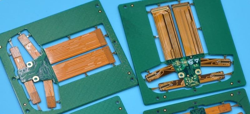
HDI Flex PCBs (High-Density Interconnector Flexible Printed Circuit Boards) are advanced circuit boards that combine high-density interconnection (HDI) technology with the flexibility of traditional flexible PCBs. HDI technology enables the creation of circuits with finer traces, microvias, and stacked vias, which are essential for compact, high-performance designs. The flexibility of these PCBs makes them ideal for applications that require space and weight savings. In the modern electronics industry, HDI Flex PCB are crucial for the miniaturization and functionality of devices. They are widely used in industries such as medical devices, where compact and reliable designs are necessary; automotive, where space-saving and durable circuits are needed for advanced control systems; consumer electronics, especially in smartphones and wearables; and aerospace, where performance and flexibility under extreme conditions are vital. HDI Flex PCBs are a key technology enabling innovation across these sectors.
What is HDI in PCB? Understanding HDI Flex PCB Technology
HDI (High-Density Interconnector) technology refers to the design and manufacturing process used to create circuit boards with high circuit density. HDI PCBs are characterized by the use of finer traces, microvias, and advanced stacking techniques that allow for increased component density in a smaller footprint. This technology is essential for applications that require highly compact, high-performance circuits. In the context of HDI Flex PCB, these designs combine HDI technology with the flexibility of traditional flex PCBs, enabling complex, high-density circuits that can bend and flex without compromising performance.
Key characteristics of HDI PCBs include:
-
Fine Lines and Spaces: HDI PCBs allow for finer traces and spaces between them, enabling the integration of more components in a smaller area.
-
Microvias: These are tiny vias (holes) used to make connections between layers. Microvias are crucial for HDI designs, allowing for higher density and more compact routing.
-
Stacked and Buried Vias: HDI PCBs often use stacked vias (vias that are drilled in multiple layers) and buried vias (vias that are hidden within layers) to further optimize space and improve signal integrity.
Compared to traditional PCBs, HDI PCBs offer significantly higher performance, greater component density, and superior design flexibility. While traditional PCBs use larger vias and traces, HDI technology allows for the creation of more intricate designs in a much smaller package. The combination of high density, miniaturization, and the flexible nature of HDI Flex PCB makes them particularly suitable for modern electronic devices that demand high performance in compact spaces.
Understanding Flex PCBs: The Backbone of HDI Flex PCB Technology
Flexible PCBs, often referred to as HDI Flex PCBs when paired with high-density interconnection technology, are circuit boards made from flexible materials that allow the board to bend, twist, and fold while maintaining its electrical integrity. Unlike traditional rigid PCBs, which are made from solid, inflexible substrates like fiberglass, HDI Flex PCBs use materials that enable the board to be used in dynamic or compact spaces where traditional rigid boards cannot be employed effectively.
The basic design elements of flexible PCBs include:
-
Flexible Substrates: These are the materials that form the base of a flex PCB. Typically, flexible PCBs use substrates made from polymers like polyimide or PET (Polyethylene Terephthalate). These materials are chosen for their flexibility, durability, and resistance to high temperatures.
-
Flexible Copper: Just like rigid PCBs, flex PCBs require copper for the conductive traces. However, for HDI Flex PCB designs, this copper is applied to the flexible substrate in such a way that it maintains both flexibility and electrical performance under bending and twisting conditions.
-
Coverlay: A flexible PCB often features a thin, protective layer known as a coverlay. This serves to protect the copper traces from damage while maintaining the board’s flexibility.
Advantages of Flexible PCBs Over Traditional Rigid PCBs
HDI Flex PCBs offer several distinct advantages over their rigid counterparts, making them an ideal choice for many modern electronic devices:
-
Weight and Space Efficiency: Because flexible PCBs can be bent and shaped to fit the available space in a device, they help reduce the overall size and weight of the product. This is particularly important for portable electronics like smartphones, wearables, and medical devices, where size and weight are critical considerations.
-
Durability and Reliability: Flexible PCBs can withstand bending and vibrations without breaking or cracking, which is a major advantage in applications that require reliability in dynamic or harsh environments. The use of HDI Flex PCB technology further enhances durability by incorporating high-density interconnections, which helps improve the robustness of these circuits.
-
Design Flexibility: The ability to shape the PCB into various forms and configurations gives designers much more freedom in product design. Flexible PCBs allow for tighter layouts and can be routed in ways that traditional rigid PCBs cannot, especially in confined or complex spaces.
Incorporating HDI Flex PCB technology into flexible PCBs enhances these benefits by allowing for even higher densities of components and circuits, making them perfect for cutting-edge applications in medical, aerospace, automotive, and consumer electronics industries.
HDI Flex PCB: Combining Two Advanced Technologies for Superior Performance
HDI Flex PCB represents the fusion of two cutting-edge technologies: High-Density Interconnection (HDI) and flexible printed circuit board (Flex PCB) technology. Each of these technologies brings its own unique advantages, but when combined, they create a powerful solution that meets the ever-increasing demands of modern electronic devices. Let’s explore how HDI and Flex technology work together and the benefits this synergy offers.
How HDI and Flex Technology Work Together
At the core of HDI Flex PCB is the integration of HDI’s dense circuit design with the inherent flexibility of traditional flex PCBs. HDI technology enhances the traditional flexible PCB by introducing microvias, fine lines, and stacked vias, which allow for higher circuit density in a smaller space. This is especially crucial for modern devices where minimizing size while maintaining functionality is paramount.
In a typical HDI Flex PCB design, the flexibility of the substrate allows the circuit board to be bent and shaped to fit tight spaces, while HDI technology allows for intricate, high-density interconnections that were previously impossible to achieve with standard flex PCBs. The combination of these technologies enables designers to create highly compact and lightweight solutions without sacrificing performance or reliability.
The Synergy of HDI’s High-Density Interconnection and the Flexibility of the PCB
The true synergy of HDI Flex PCB lies in the unique balance between HDI’s high-density interconnection and the flexibility of the PCB. On one hand, HDI’s ability to route more components and connections in a limited space enables the creation of high-performance circuits, even in extremely small form factors. On the other hand, the flexibility of the PCB allows for a more versatile design that can bend, twist, and fit into irregular or constrained spaces—something traditional rigid PCBs cannot achieve.
This synergy is particularly useful for applications like wearables, where space is at a premium, or in medical devices that require both high performance and flexibility. HDI Flex PCB allows for sophisticated circuit designs that need to perform reliably in dynamic environments while taking up minimal space.
The Benefits of Combining HDI with Flex: Compact Design, Improved Performance, and Reliability
Combining HDI with Flex technology in HDI Flex PCBs offers several key benefits that make them indispensable in the modern electronics landscape:
-
Compact Design: The small size and flexibility of HDI Flex PCBs make them ideal for devices where space-saving is crucial. Designers can create smaller, more efficient products without sacrificing performance. The ability to bend or fold the PCB also enables complex shapes and space-efficient routing, which is essential in tight or curved spaces.
-
Improved Performance: HDI technology improves the signal integrity and reduces the chance of interference, ensuring better performance even at high frequencies. The dense routing capabilities of HDI Flex PCBs provide greater circuit density, meaning more components can be integrated into a smaller board while maintaining high-speed signal integrity. This leads to better overall performance for the device.
-
Reliability: The combination of HDI Flex PCB provides exceptional reliability. Flexible substrates are highly durable and can withstand stresses such as bending, vibration, and thermal fluctuations without cracking or breaking. This is critical in mission-critical applications such as aerospace, automotive, and medical devices. The precision and performance of HDI also ensure that the connections are robust and less prone to failure.
The fusion of HDI’s high-density interconnections and the flexible nature of HDI Flex PCBs results in an ideal solution for advanced electronics that require both compactness and superior performance. Whether it’s for consumer electronics, industrial devices, or high-tech medical equipment, this combination delivers a powerful, versatile, and reliable solution that meets the demands of modern, cutting-edge applications.
Key Features of HDI Flex PCB: Unlocking High-Performance Design
HDI Flex PCBs combine advanced features that enable high-density, reliable, and flexible circuit designs. These features, from microvias to high-speed performance capabilities, make HDI Flex PCBs essential for modern electronic devices where space, speed, and functionality are paramount. Let’s explore the key characteristics that define HDI Flex PCBs and their role in advanced electronic applications.
Microvias and Blind/Buried Vias: Enabling High-Density Interconnections
One of the most crucial features of HDI Flex PCBs is the use of microvias—small holes drilled into the PCB to establish electrical connections between layers. Microvias are particularly important for creating dense interconnections within a limited space, allowing for HDI Flex PCBs to pack more components into smaller areas without sacrificing functionality.
In addition to microvias, HDI Flex PCBs often incorporate blind vias (vias that only connect the outer layers to one or more inner layers) and buried vias (vias that connect layers but are not visible from the outside of the PCB). These types of vias enable more efficient use of space by reducing the number of through-hole vias, which would otherwise take up valuable surface area. The combination of these via types ensures that HDI Flex PCBs maintain both high-density interconnections and structural flexibility, which are critical in modern applications where performance and miniaturization are key.
Layer Counts: Common Layer Configurations for HDI Flex PCBs
Another defining feature of HDI Flex PCBs is their ability to support a range of layer counts, which determines the complexity and functionality of the PCB. HDI Flex PCBs can be fabricated with various layer configurations depending on the specific needs of the application.
-
4-Layer HDI Flex PCBs: These are among the most common configurations, offering a good balance of performance and cost-effectiveness. The four layers allow for complex routing of signals while maintaining flexibility and compactness.
-
6-Layer HDI Flex PCBs: For more advanced applications, 6-layer configurations offer greater complexity and the ability to handle more components and higher-density interconnections. These are often used in high-performance devices like smartphones and wearables.
-
Multilayer HDI Flex PCBs: For the most complex applications, HDI Flex PCBs can be fabricated with more than six layers. These multilayer designs enable the integration of numerous circuits and components in even smaller spaces, which is essential for devices requiring high-performance, such as medical equipment, aerospace systems, and advanced consumer electronics.
The ability to support multiple layers while maintaining flexibility allows HDI Flex PCBs to cater to a wide range of applications, from simple devices to highly sophisticated electronics.
High-Speed Performance: Meeting the Demands of High-Frequency Signals
As electronic devices continue to become more complex and demanding, high-speed performance is more critical than ever. HDI Flex PCBs are specifically designed to handle high-frequency signals, ensuring that data can be transmitted quickly and efficiently across all layers of the PCB.
By utilizing HDI Flex PCB technology, designers can achieve low signal loss and reduced interference, which is vital for applications requiring fast data transfer rates. Microvias, precise layer stacking, and advanced signal routing techniques are employed in HDI Flex PCBs to reduce the path length and minimize impedance mismatches. These design strategies ensure that HDI Flex PCBs deliver optimal performance in high-frequency environments, such as in 5G communications, high-performance computing, and other advanced electronics that require rapid signal processing.
Miniaturization: Reducing Size and Weight for Modern Electronics
Miniaturization is one of the most significant benefits of HDI Flex PCBs. The ability to pack a high density of circuits into a small form factor allows HDI Flex PCBs to play a critical role in the development of lightweight, compact devices. The small size and flexibility of HDI Flex PCBs make them ideal for industries where space and weight are limited, such as in wearable electronics, medical implants, automotive applications, and portable devices.
By combining the high-density capabilities of HDI with the flexible nature of the PCB, HDI Flex PCBs enable designers to reduce the overall size and weight of their products without compromising on performance or durability. This is crucial for modern electronics, where consumers and industries alike demand sleek, efficient, and high-performance devices that do not sacrifice portability.
The key features of HDI Flex PCBs, from microvias and advanced layer configurations to high-speed performance and miniaturization, make them an essential technology for today’s high-performance electronics. Whether it’s for creating space-efficient devices or ensuring reliable performance in demanding environments, HDI Flex PCBs offer unparalleled flexibility, density, and speed, helping to drive innovation in industries ranging from consumer electronics to aerospace and medical applications.
HDI Flex PCB Applications: Transforming Industries with High-Performance Flexibility
HDI Flex PCBs have become an indispensable component in a wide array of industries due to their unique combination of high-density interconnections and flexible, compact design. These advanced circuit boards are utilized in applications that require performance, miniaturization, and reliability. Let’s take a closer look at the diverse industries where HDI Flex PCBs play a critical role.
Consumer Electronics: Revolutionizing Smartphones, Tablets, and Wearables with HDI Flex PCB
In the realm of consumer electronics, HDI Flex PCBs are at the forefront of innovation. Devices like smartphones, tablets, and wearables demand ultra-compact, high-performance circuit boards that can handle increasingly complex functions while saving space and weight. HDI Flex PCBs allow for smaller, lighter designs, which is crucial for portable devices that require flexibility, durability, and high-speed performance.
For smartphones and tablets, the integration of HDI Flex PCBs enables manufacturers to include more features in a thinner package without compromising signal integrity or power efficiency. Wearables, such as smartwatches and fitness trackers, benefit from the flexibility of these PCBs, allowing for flexible, curved, and lightweight designs that can be comfortably worn on the body while still maintaining high performance. The ability to bend and fold these PCBs without losing functionality is a game changer for compact, wearable technology.
Medical Devices: Enhancing Performance with HDI Flex PCB Technology
The medical device industry is another area where HDI Flex PCBs have a significant impact. Medical electronics often require devices that are not only compact and lightweight but also highly reliable and capable of functioning in demanding, real-time applications. From implantable devices to diagnostic equipment, HDI Flex PCBs are used to create small, efficient, and highly reliable solutions that can perform under extreme conditions.
For example, HDI Flex PCBs are crucial in pacemakers, hearing aids, and other medical implants, where size and flexibility are of utmost importance. The high-density interconnections of HDI Flex PCBs allow for the integration of more components in smaller spaces, which is critical for medical devices that need to be as small and as effective as possible. Additionally, the flexibility of these PCBs helps ensure that the devices can function within the body or other tight environments.
Automotive Electronics: Enhancing Automotive Systems with HDI Flex PCBs
The automotive industry has embraced HDI Flex PCBs due to the increasing demand for more advanced electronic systems in vehicles. These systems include everything from advanced driver assistance systems (ADAS) to infotainment systems, sensors, and control units. As cars become smarter, more connected, and more autonomous, the need for efficient, high-density, and flexible circuit boards grows.
HDI Flex PCBs play an essential role in automotive electronics by offering solutions that are both space-efficient and highly reliable in harsh automotive environments. The flexibility of these PCBs allows for innovative designs in tight spaces, while the high-density capabilities enable the integration of numerous functions into a small, lightweight board. Additionally, HDI Flex PCBs are well-suited to withstand the challenging conditions of temperature variations, vibrations, and other stresses commonly encountered in the automotive industry.
Aerospace and Military: The Use of HDI Flex PCB in Harsh Environments
In the aerospace and military industries, HDI Flex PCBs are used in applications that demand extreme performance and reliability. These sectors require electronic systems that can endure harsh conditions, such as extreme temperatures, vibration, and exposure to radiation. HDI Flex PCBs provide the perfect solution, offering durability, high-density connections, and the ability to function in confined spaces.
In aerospace, HDI Flex PCBs are employed in systems like flight control, navigation, communication, and satellite technology, where space is limited and performance is critical. For military applications, HDI Flex PCBs are used in a variety of systems, including weapons, drones, and communication devices, where both the flexibility of the PCB and its ability to handle high-performance requirements in extreme conditions are essential.
Industrial Applications: Powering Robotics, Sensors, and IoT Devices with HDI Flex PCB
HDI Flex PCBs are increasingly being adopted in industrial applications, particularly in robotics, sensors, and IoT devices. The miniaturization and high-density capabilities of HDI Flex PCBs make them ideal for devices that need to be compact, reliable, and capable of handling complex functions within tight spaces.
In robotics, HDI Flex PCBs allow for smaller, lighter robots with more advanced electronic systems. The flexibility of the PCB enables robots to move and function in environments where rigid PCBs might fail. Similarly, in sensor technology, HDI Flex PCBs provide a compact and efficient platform for sensors used in manufacturing, monitoring, and safety systems. The flexibility and density of these PCBs help reduce the size and weight of sensors while enhancing their performance and reliability.
For IoT devices, which often require tiny, low-power, and reliable circuit boards, HDI Flex PCBs enable the creation of devices that can be seamlessly integrated into various applications, from smart homes to industrial automation. The ability to pack more components into a smaller area while maintaining flexibility is a significant advantage for the growing field of IoT.
The diverse applications of HDI Flex PCBs demonstrate their importance across multiple industries. Whether it’s in consumer electronics, medical devices, automotive systems, aerospace, or industrial applications, HDI Flex PCBs offer the ideal combination of flexibility, high-density performance, and reliability. As the demand for compact, high-performance devices continues to grow, HDI Flex PCBs will remain at the forefront of technological innovation, enabling more efficient, smaller, and smarter electronic solutions.
HDI Flex PCB Manufacturing Process: Detailed Steps and Key Considerations
The HDI Flex PCB manufacturing process combines several advanced techniques that allow for the creation of high-density, flexible circuit boards. This process is more intricate than traditional rigid PCB fabrication due to the flexible substrates and complex layer interconnections required for HDI Flex PCBs. Below, we’ll explore an overview of the fabrication steps involved in producing HDI Flex PCBs, how it differs from rigid PCB manufacturing, and the key considerations that ensure the quality and reliability of the final product.
Overview of the Fabrication Steps for HDI Flex PCB
The manufacturing of HDI Flex PCBs generally involves the following steps:
-
Material Preparation: The process begins with selecting the appropriate flexible substrate, typically made from polymers like polyimide or PET (Polyethylene Terephthalate). These materials provide the required flexibility, durability, and resistance to heat and chemicals. The copper foil, which serves as the conductive layer, is laminated onto the flexible substrate.
-
Layer Stacking: For multilayer HDI Flex PCBs, the next step involves stacking the layers that will form the final PCB. These layers may include copper traces, vias, and insulating material. The layers are carefully aligned, and adhesives are applied to bond them together.
-
Circuit Patterning: The desired circuit pattern is then created on the copper layer using photolithography. A photoresist is applied to the copper surface, and ultraviolet (UV) light is used to expose the circuit design. The areas that are exposed are then etched away, leaving behind the desired conductive traces.
-
Microvia Drilling: One of the defining features of HDI Flex PCBs is the use of microvias—tiny holes that connect the different layers of the PCB. These are typically created using laser drilling, a precise method that allows for the creation of small, high-density vias. Microvias are key to achieving the compact design and high-density interconnections that HDI Flex PCBs are known for.
-
Via Formation: In addition to microvias, HDI Flex PCBs often use blind and buried vias for connecting different layers of the PCB. These vias are formed using specialized techniques, which allow them to be either partially visible (blind vias) or completely hidden within the layers of the PCB (buried vias). Via formation is one of the most critical steps in ensuring the high-density interconnections that make HDI Flex PCBs effective in high-performance applications.
-
Plating and Metallization: After the vias are formed, the copper inside the vias is plated using electroplating techniques. This step ensures that the vias are electrically conductive and capable of carrying signals between the different layers. For HDI Flex PCBs, the plating process must be precise to ensure the reliable electrical performance of the PCB.
-
Coverlay Application: A protective layer, called the coverlay, is applied over the flexible substrate to protect the copper traces and prevent damage during handling and use. The coverlay is typically made of a flexible, transparent material like polyimide, which allows the board to retain its flexibility while offering protection.
-
Final Testing and Inspection: Once the fabrication process is complete, HDI Flex PCBs undergo rigorous testing to ensure they meet all design specifications and function correctly. This includes electrical testing, visual inspection, and sometimes advanced techniques like X-ray inspection for internal vias. The boards are also subjected to mechanical testing to ensure they can withstand bending and flexing without failure.
Differences Between Rigid PCB and HDI Flex PCB Manufacturing
The manufacturing process for HDI Flex PCBs differs from traditional rigid PCB fabrication in several key aspects:
-
Substrate Materials: The most obvious difference is the use of flexible substrates like polyimide or PET for HDI Flex PCBs, compared to rigid materials like fiberglass-reinforced epoxy (FR4) used in traditional PCBs. This change in material affects the way the boards are handled, processed, and treated during fabrication.
-
Layer Handling and Bonding: In rigid PCB manufacturing, the layers are stacked and bonded using heat and pressure, which is a straightforward process. For HDI Flex PCBs, however, the layers are laminated onto the flexible substrate with careful consideration for the flexibility and durability of the final product.
-
Via Formation: The via formation process is also different. While traditional rigid PCBs use larger through-holes, HDI Flex PCBs often rely on microvias, blind vias, and buried vias, which are drilled using lasers with high precision. This allows for higher-density designs in a more compact space, something not achievable with conventional rigid PCB designs.
-
Coverlay and Protection: HDI Flex PCBs require a protective coverlay layer that is applied to the flexible substrate to ensure the copper traces are protected during bending or stretching. Traditional rigid PCBs, on the other hand, typically use solder masks and do not require flexible coverlays.
Key Considerations for the Fabrication of HDI Flex PCB
Several key factors need to be carefully considered when manufacturing HDI Flex PCBs to ensure optimal performance and reliability:
-
Material Choices: The selection of materials for HDI Flex PCBs is critical. The substrate material must offer the right combination of flexibility, thermal stability, and electrical performance. Polyimide is commonly used due to its high heat resistance and flexibility, while PET may be used for lower-cost applications. The copper foil used for the conductive traces must also be chosen carefully to ensure it bonds well with the flexible substrate and can withstand the stress of bending and flexing.
-
Via Formation and Design: The precision in drilling microvias and forming blind and buried vias is crucial for the performance of HDI Flex PCBs. The vias must be small enough to achieve high-density interconnections without compromising the structural integrity of the PCB. The via design also needs to account for the flexibility of the PCB, ensuring that the vias do not create weak points that could fail during bending.
-
Thermal Management: HDI Flex PCBs often operate in environments with varying temperatures. Effective thermal management is essential to prevent overheating, especially in high-performance applications like automotive and aerospace electronics. The materials used must be capable of dissipating heat without degrading the flexibility of the PCB.
-
Electrical Performance: As HDI Flex PCBs are often used in high-speed and high-frequency applications, the electrical performance must be top-notch. This includes ensuring low signal loss, minimizing impedance mismatches, and optimizing the via design to handle high-speed signals.
-
Reliability Testing: Given the flexible nature of HDI Flex PCBs, reliability testing is even more critical. The board must be tested for its ability to withstand repeated flexing, bending, and exposure to environmental stresses. This includes testing for fatigue, thermal cycling, and other mechanical stresses to ensure long-term reliability.
The manufacturing process for HDI Flex PCBs involves a range of specialized techniques, from selecting the right materials to forming microvias and applying protective coverlays. It differs significantly from traditional rigid PCB manufacturing, with a stronger emphasis on flexibility, high-density interconnections, and precision. By understanding the fabrication steps and key considerations, manufacturers can produce HDI Flex PCBs that meet the demands of high-performance applications while maintaining reliability and durability. As technology continues to evolve, the role of HDI Flex PCBs will only become more critical in driving innovation across multiple industries.
Advantages of HDI Flex PCB: Unlocking Space Efficiency, Flexibility, and Reliability
HDI Flex PCBs are engineered to meet the needs of modern, high-performance electronic systems. With their combination of advanced features like high-density interconnections and flexible substrates, HDI Flex PCBs offer significant advantages in terms of space efficiency, flexibility, reliability, and heat dissipation. Below, we explore these key benefits in greater detail, illustrating how HDI Flex PCBs stand out in a variety of demanding applications.
Space Efficiency: Maximizing Compact Designs
One of the most compelling advantages of HDI Flex PCBs is their ability to save space, making them perfect for compact designs. In industries where size and weight are critical—such as in wearables, smartphones, or medical devices—the ability to fit more components into a smaller area is invaluable.
The high-density interconnection (HDI) technology allows for much more efficient use of space compared to traditional rigid PCBs. By incorporating features such as microvias and stacked vias, HDI Flex PCBs can support complex circuit designs while maintaining a small footprint. The flexible nature of the PCB also allows for more creative packaging and integration, where the circuit board can be bent or shaped to fit around other components, further saving valuable space. This is particularly useful for applications where there are limited design constraints, such as in wearable electronics, IoT devices, and compact consumer gadgets.
Flexibility and Durability: Adaptability for Dynamic Applications
The inherent flexibility of HDI Flex PCBs is a game changer in applications where traditional rigid PCBs cannot perform well. Flexibility enables the PCB to bend and conform to non-flat surfaces, providing greater design freedom and adaptability. This makes HDI Flex PCBs ideal for use in products that must be flexible or undergo physical movement during operation.
For example, in medical devices like flexible implants or wearables like smartwatches, HDI Flex PCBs can bend with the body, reducing discomfort and ensuring that the device remains functional despite continuous movement. Their durability in bending ensures that the circuits can withstand repeated flexing without the risk of failure, something that would be a concern for rigid PCBs. This property is also important in robotics, where the PCB may need to flex as part of the robotic structure.
In addition to flexibility, HDI Flex PCBs are incredibly durable. The use of materials like polyimide provides excellent resistance to mechanical stress, ensuring that the PCB can endure harsh physical environments and maintain high performance over time. This combination of flexibility and durability makes HDI Flex PCBs a preferred choice for dynamic applications where reliability is a top priority.
Reliability: Superior Performance for Mission-Critical Applications
When it comes to mission-critical applications—such as those in aerospace, automotive, and medical devices—reliability is non-negotiable. HDI Flex PCBs offer superior reliability compared to traditional rigid PCBs, particularly in environments where mechanical stresses, temperature fluctuations, and vibrations are prevalent.
The flexibility of HDI Flex PCBs allows them to better withstand mechanical stress, such as bending, twisting, or vibration, without compromising their electrical performance. In aerospace applications, for instance, HDI Flex PCBs are used in avionics and satellite systems, where reliability and performance are essential in extreme conditions. Similarly, in automotive electronics, HDI Flex PCBs provide a level of flexibility and resistance to environmental challenges that traditional rigid PCBs simply cannot match.
The high-density nature of HDI Flex PCBs also contributes to their reliability by allowing for tightly packed circuits with fewer potential points of failure. Microvias and stacked vias enable complex circuits to be integrated with a higher degree of precision, reducing the chances of faults. Additionally, HDI Flex PCBs are often subjected to rigorous testing, including thermal cycling, vibration, and mechanical stress tests, to ensure they can perform reliably over long periods in demanding environments.
Heat Dissipation: Efficient Thermal Management for Enhanced Performance
Thermal management is a critical aspect of PCB design, particularly in high-performance systems where heat buildup can negatively affect the operation and longevity of electronic components. HDI Flex PCBs offer superior heat dissipation capabilities compared to traditional rigid PCBs, making them ideal for high-frequency, high-power applications.
The combination of flexible materials and high-density interconnections in HDI Flex PCBs allows for more efficient spreading of heat across the surface of the PCB. This capability is particularly important in devices like smartphones, automotive electronics, and power electronics, where components may generate significant amounts of heat. The use of materials like polyimide in HDI Flex PCBs helps improve heat resistance, allowing the PCB to operate effectively at higher temperatures without risk of failure.
The thin, flexible nature of HDI Flex PCBs allows for better thermal conduction by minimizing thermal resistance. In applications such as LED lighting or electric vehicles, where heat management is a top priority, the ability of HDI Flex PCBs to dissipate heat more effectively helps ensure that devices remain cool and perform optimally, even under heavy loads.
The advantages of HDI Flex PCBs—from space efficiency and flexibility to superior reliability and heat dissipation—make them an ideal choice for modern electronics. Their ability to integrate high-density interconnections in a compact, flexible format allows them to excel in a variety of applications, including wearables, medical devices, automotive systems, aerospace technology, and industrial robots. As the demand for smaller, more efficient, and higher-performing devices continues to grow, HDI Flex PCBs will remain at the forefront of technological innovation, enabling the development of next-generation electronics with exceptional performance and reliability.
Challenges and Limitations of HDI Flex PCB: Navigating Cost, Manufacturing, and Design Complexities
While HDI Flex PCBs offer significant advantages in terms of performance, flexibility, and space efficiency, they also come with their own set of challenges and limitations. These challenges, often related to cost, manufacturing complexity, and design intricacies, need to be carefully addressed to ensure that HDI Flex PCBs meet the stringent requirements of high-performance applications. Below, we explore the key challenges faced during the development and production of HDI Flex PCBs, as well as the strategies used to mitigate these issues.
Cost Considerations: Impact of Design Complexity on Expenses
One of the primary challenges of HDI Flex PCBs is their cost, which can be significantly higher than traditional rigid PCBs. The higher costs are largely due to the complexity of HDI Flex PCB designs and the advanced manufacturing techniques required to produce them.
-
Material Costs: HDI Flex PCBs use advanced flexible substrates such as polyimide, which tend to be more expensive than traditional rigid materials like FR4. These materials offer superior flexibility and thermal resistance, but they also increase the overall cost of the PCB.
-
Manufacturing Complexity: The processes used to fabricate HDI Flex PCBs—such as laser drilling for microvias, layer stacking, and via formation (blind and buried vias)—require highly specialized equipment and advanced technology. These processes are more time-consuming and require higher precision, which leads to increased production costs.
-
Higher Yield Loss: Due to the complexity and precision required in HDI Flex PCB fabrication, there may be a higher yield loss during production, especially if the manufacturing process is not closely monitored. This contributes to higher costs per unit, as defective boards must be discarded or reworked.
-
Design Complexity: As the design of HDI Flex PCBs incorporates high-density interconnections, it requires more intricate planning and layout work. The increased design time and expertise needed add to the overall cost of the project.
While HDI Flex PCBs provide value through enhanced performance, their cost can be a barrier for some applications, especially in price-sensitive markets. However, as technology improves and manufacturing techniques become more streamlined, the cost of HDI Flex PCBs is expected to decrease over time, making them more accessible to a wider range of industries.
Manufacturing Challenges: Ensuring Precision in High-Density and Flexible Designs
The manufacturing of HDI Flex PCBs is a delicate and complex process, requiring high precision at every stage to ensure that the final product meets performance expectations. Several challenges must be overcome during production:
-
Microvia and Via Formation: One of the key features of HDI Flex PCBs is the use of microvias—tiny holes that provide high-density interconnections between layers. Creating these vias with such small dimensions requires advanced laser drilling technology. Achieving consistent via size and placement is critical, and any variation can compromise the integrity of the circuit. Additionally, the formation of blind and buried vias adds another layer of complexity to the manufacturing process.
-
Layer Alignment: As HDI Flex PCBs often use multiple layers, ensuring precise alignment during the lamination process is essential. Misalignment can lead to poor electrical performance, connection failures, or even complete functional failure of the PCB.
-
Handling of Flexible Materials: The flexible substrates used in HDI Flex PCBs can be more challenging to handle during manufacturing compared to rigid materials. Flexible substrates are more susceptible to damage from mechanical stress or heat, and care must be taken during all stages of production to avoid compromising the board’s integrity. This increases the difficulty of achieving consistently high-quality results.
-
Thin Trace and Via Sizes: HDI Flex PCBs are designed to support high-density circuits with fine traces and small vias. The precision required to manufacture these tiny features demands state-of-the-art equipment and skilled operators. Variations in trace width or via size can lead to signal integrity issues or even complete circuit failures.
Manufacturing HDI Flex PCBs requires significant expertise, high-tech equipment, and strict quality control measures to achieve the necessary precision and reliability. Any deviation in the manufacturing process can impact the final product, making it crucial to address these challenges to maintain product quality.
Design Complexity: Ensuring High-Quality and Functional HDI Flex PCB
Designing an HDI Flex PCB is a highly specialized task that requires in-depth knowledge of both flexible circuit design and high-density interconnection technologies. Several design considerations must be addressed to ensure the HDI Flex PCB meets performance, functionality, and reliability requirements.
-
Layer Stackup and Via Design: Since HDI Flex PCBs often include multiple layers, the design of the layer stackup is a critical aspect of the design process. The designer must ensure that the via structure—whether it’s blind, buried, or microvia—is appropriately chosen to ensure efficient signal routing and reliable electrical performance. Each layer’s impedance and interaction with adjacent layers must also be considered to avoid signal integrity issues, especially in high-frequency applications.
-
Bend Radius and Flexibility Considerations: The flexible nature of HDI Flex PCBs means that designers must carefully account for the PCB’s intended bending radius during the design process. Excessive bending or torsion beyond the specified limits can cause mechanical damage to the PCB, leading to failure. The material selection, trace width, and via design must be optimized to withstand the mechanical stresses that come with repeated bending.
-
Signal Integrity and High-Frequency Performance: As HDI Flex PCBs are often used in high-performance applications (e.g., telecommunications, automotive, or medical electronics), ensuring signal integrity is paramount. Designers must account for factors such as impedance matching, trace width, and via configuration to minimize signal loss and reduce electromagnetic interference (EMI). The high-density nature of the board, combined with the flexible substrate, requires precise engineering to maintain optimal performance.
-
Thermal Management: The thin, flexible nature of HDI Flex PCBs can present challenges in terms of heat dissipation. While flexible PCBs are often used in high-performance applications, designers need to consider heat management strategies to prevent overheating of components. Heat spreading can be more difficult in HDI Flex PCBs compared to traditional rigid PCBs, which can lead to thermal stress and potential component failure. Design engineers need to integrate efficient heat dissipation strategies, such as heat sinks or copper pours, to mitigate these challenges.
-
Testability and Quality Assurance: Testing HDI Flex PCBs can be more challenging than testing traditional rigid PCBs. The flexible nature of the board may make it difficult to use traditional testing methods, such as fixture-based testing or in-circuit testing. Designers need to ensure that test points are accessible and that the design allows for efficient and effective testing of the PCB’s electrical and mechanical properties.
While HDI Flex PCBs offer numerous advantages in terms of compact design, flexibility, and high-performance capabilities, they also come with significant challenges that need to be addressed during the design and manufacturing phases. The complexity of the design process, the need for precision in manufacturing, and the higher costs associated with these advanced PCBs are key considerations that must be factored into any project involving HDI Flex PCBs. However, by leveraging the right expertise, tools, and manufacturing techniques, these challenges can be effectively managed, enabling the development of high-quality, reliable HDI Flex PCBs that meet the demanding requirements of modern electronics.
HDI Flex PCB Cost: Understanding the Pricing Factors and Estimation Tools
The cost of HDI Flex PCBs can vary widely depending on several key factors, such as layer count, material selection, and design complexity. As an advanced type of flexible printed circuit board (PCB), HDI Flex PCBs are typically more expensive than traditional flex PCBs due to their high-density interconnection technology and the sophisticated manufacturing processes involved. Understanding the key factors that influence the cost of HDI Flex PCBs can help companies make informed decisions about their designs and budgets. This section delves into these cost drivers, compares the cost of HDI Flex PCBs to traditional flex PCBs, and introduces tools and calculators that can help estimate costs more accurately.
Factors Influencing the Cost of HDI Flex PCB
The cost of manufacturing HDI Flex PCBs is influenced by a variety of factors. Each factor can contribute significantly to the overall price of the PCB, and designers must account for these elements when planning their projects.
-
Layer Count: One of the most important factors affecting the cost of HDI Flex PCBs is the number of layers in the design. More layers require additional processing steps, including lamination, drilling, and via formation, which increases both the time and the materials needed to complete the PCB. As the complexity of the design grows with more layers (such as 4-layer or 6-layer HDI Flex PCBs), so does the cost. Higher layer counts also require precision alignment, which adds to manufacturing costs. This makes HDI Flex PCBs with multiple layers more expensive than simpler designs.
-
Material Selection: The materials chosen for HDI Flex PCBs play a crucial role in determining cost. Flexible substrates, such as polyimide or PET (Polyethylene Terephthalate), are more expensive than standard rigid materials like FR4. Polyimide, in particular, is favored for its excellent heat resistance and flexibility, but it drives up the material costs. Additionally, the quality of copper used for the PCB traces and the type of laminate for the insulating layers can also impact the overall price. Materials that are optimized for high-frequency or high-thermal applications tend to cost more due to their advanced properties.
-
Design Complexity: HDI Flex PCBs typically incorporate advanced features such as microvias, blind vias, buried vias, and fine traces. These design elements require specialized equipment and expertise, driving up costs. For example, the process of creating microvias is more intricate and expensive than standard via formation in traditional PCBs. Additionally, high-density designs require precise manufacturing to ensure signal integrity and reliability, further contributing to the overall cost. More complex designs often require longer lead times, which can increase costs due to additional labor and testing requirements.
-
Volume: The volume of HDI Flex PCB production plays a significant role in cost. Typically, HDI Flex PCBs are more expensive to produce in smaller quantities due to setup costs and the need for specialized equipment. Higher-volume orders allow for economies of scale, reducing the per-unit cost. However, even in high-volume production, HDI Flex PCBs remain more expensive than traditional flex PCBs due to the advanced technology and materials involved.
How HDI Flex PCB Costs Compare to Traditional Flex PCBs
When comparing HDI Flex PCBs to traditional flex PCBs, the cost disparity is evident. Traditional flex PCBs are typically simpler in design and have fewer layers, which makes them more cost-effective to manufacture. They also often use more standard materials, which are less expensive than those required for HDI Flex PCBs.
HDI Flex PCBs are designed for more complex applications that demand high-density interconnections, miniaturization, and greater electrical performance. As a result, they require advanced manufacturing processes, more specialized materials, and higher precision during production, all of which contribute to the increased cost. The need for microvias, stacked vias, and fine traces in HDI Flex PCBs also increases the cost, as these features require advanced technologies like laser drilling and precision alignment that are not necessary for traditional flex PCBs.
HDI Flex PCBs are more expensive than traditional flex PCBs due to the added complexity in both the design and manufacturing processes. However, they offer substantial performance benefits, such as higher density, better signal integrity, and greater durability, which may justify the additional cost in applications where these factors are critical, such as in medical devices, aerospace systems, and high-performance consumer electronics.
Tools and Calculators Available for Estimating HDI Flex PCB Costs
Estimating the cost of HDI Flex PCBs can be a complex task due to the variety of factors involved. Fortunately, several tools and calculators are available to help companies and engineers estimate costs more accurately and plan their budgets effectively.
-
Hemeixin HDI Flex PCB Cost Calculator: The Hemeixin HDI Flex PCB Cost Calculator is a popular online tool that helps users estimate the cost of HDI Flex PCBs based on their specific design requirements. This calculator takes into account factors such as layer count, material selection, via types, and production volume to generate a cost estimate. By inputting the necessary parameters, users can quickly gain insights into the expected cost of their HDI Flex PCBs, making it easier to compare prices and make informed decisions about their projects.
-
PCB Manufacturer’s Online Tools: Many PCB manufacturers, including those that specialize in HDI Flex PCBs, offer online cost calculators that provide real-time pricing based on the design specifications. These tools can help estimate costs based on parameters such as the number of layers, trace width, and material type. Some calculators also allow users to upload their PCB designs and receive a more accurate cost estimate.
-
Design and Manufacturing Quotes: In addition to cost calculators, it is advisable to request quotes from PCB manufacturers directly. This can provide a more tailored cost estimate based on your unique design and requirements. Some manufacturers may offer volume discounts, prototype pricing, or cost optimization suggestions that can help reduce the overall cost of HDI Flex PCBs.
The cost of HDI Flex PCBs is influenced by several factors, including layer count, material selection, design complexity, and production volume. While HDI Flex PCBs are generally more expensive than traditional flex PCBs due to their advanced technology and manufacturing processes, they offer significant benefits in terms of high-density interconnections, miniaturization, and electrical performance. By using cost estimation tools like the Hemeixin HDI Flex PCB Cost Calculator and consulting with PCB manufacturers, designers can better understand the pricing structure and plan their budgets accordingly. Despite the higher upfront costs, HDI Flex PCBs are often worth the investment for applications that require high performance, reliability, and space efficiency.
Are HDI Flex PCB Reliable? Ensuring Durability and Performance
Reliability is one of the most important factors when evaluating the suitability of HDI Flex PCBs for high-performance applications. These advanced circuit boards are designed to offer superior electrical performance, compactness, and flexibility. However, ensuring their reliability requires careful attention to material choices, manufacturing quality, environmental factors, and design strategies. This section delves into the key factors that affect the reliability of HDI Flex PCBs, provides design tips for maximizing their durability, and outlines best practices for ensuring long-term performance in real-world applications.
Factors Affecting the Reliability of HDI Flex PCB
Several factors play a significant role in determining the reliability of HDI Flex PCBs. Understanding these factors is essential for designing and manufacturing durable and high-performing boards.
-
Material Choices: The selection of materials used in HDI Flex PCBs is a critical factor in determining their overall reliability. For instance, the flexible substrates used, such as polyimide, PET, or other advanced materials, need to have the right balance of flexibility, thermal resistance, and electrical properties to ensure consistent performance in dynamic environments. Low-quality materials can degrade over time, causing mechanical or electrical failures. Polyimide is a popular choice for high-performance HDI Flex PCBs because it offers excellent heat resistance and flexibility, but ensuring the quality of the material is essential for maintaining long-term reliability.
-
Manufacturing Quality: The precision with which HDI Flex PCBs are manufactured plays a significant role in their reliability. The complexity of HDI Flex PCBs—with features like microvias, stacked vias, and fine traces—requires high-precision manufacturing processes. Any misalignment during the lamination or via formation stages can lead to weak electrical connections or circuit failure. Additionally, the handling of the flexible materials during production must be done carefully to avoid introducing mechanical stress, which can lead to cracking or delamination. The quality of manufacturing processes, such as laser drilling for microvias and stacked via formation, is essential for ensuring a robust and reliable final product.
-
Environmental Conditions: HDI Flex PCBs are often used in environments where they may be exposed to extreme temperatures, moisture, vibration, or mechanical stress. The reliability of HDI Flex PCBs can be impacted by these environmental conditions. For example, high temperatures can cause thermal expansion, which can stress the connections and cause solder joints to fail. Similarly, exposure to moisture can result in corrosion, which may degrade the performance of the PCB over time. Ensuring that HDI Flex PCBs are designed to withstand these environmental factors is crucial for their reliability. Special coatings or encapsulants may be used to protect the PCB from moisture and environmental damage.
Design Tips to Ensure the Reliability of HDI Flex PCB in Real-World Applications
To ensure the reliability of HDI Flex PCBs in demanding applications, designers must focus on several key considerations during the design phase. Implementing these best practices can significantly enhance the durability and performance of the final product.
-
Consider the Bend Radius: The bend radius is the minimum radius that the HDI Flex PCB can safely bend without causing damage. When designing flexible PCBs, it’s crucial to calculate and respect the specified bend radius to avoid mechanical damage that can lead to trace fractures or delamination. The bend radius should be carefully considered based on the intended application and the material properties of the flexible substrate.
-
Choose the Right Via Types: The type of via (e.g., blind, buried, or microvia) chosen for an HDI Flex PCB design can significantly affect the reliability of the final product. Microvias, which are commonly used in HDI Flex PCBs, need to be precisely formed and well-connected to ensure optimal electrical performance. Improper via formation or poorly placed vias can lead to unreliable connections and signal integrity issues.
-
Optimizing Layer Stackup and Trace Design: When designing HDI Flex PCBs, the layer stackup and trace layout should be optimized for the intended application. Careful attention should be given to signal integrity, impedance control, and the avoidance of tight corners or sharp turns in the traces, which can weaken the electrical connections over time. In high-frequency applications, it’s especially important to ensure that the traces are designed for minimal loss and signal degradation.
-
Thermal Management: Heat dissipation is critical for the long-term reliability of HDI Flex PCBs. In high-power applications, HDI Flex PCBs must be designed with effective thermal management strategies, such as incorporating copper pours for heat spreading or adding heat sinks to critical components. Ensuring proper heat distribution can prevent thermal stresses that may lead to failure.
Best Practices for Maximizing Reliability: Insights into Design Strategies for Enhanced Durability
To further improve the durability and performance of HDI Flex PCBs, designers can implement the following best practices:
-
Use of Robust Testing and Simulation: Before manufacturing, it is essential to conduct thorough testing and simulation of the HDI Flex PCB design. This includes electromagnetic simulation to ensure signal integrity, thermal simulation to predict heat dissipation, and mechanical stress testing to assess the flexibility and durability of the board under various bending and vibration conditions. Using simulation tools early in the design process helps identify potential reliability issues and allows designers to make necessary adjustments.
-
Incorporate Redundant Design Elements: For mission-critical applications, incorporating redundant connections or redundant vias can improve the overall reliability of the HDI Flex PCB. Redundancy ensures that if one via or connection fails, the other can take over, minimizing the risk of a complete failure.
-
Apply Protective Coatings: Using conformal coatings or encapsulants can protect HDI Flex PCBs from environmental damage, including moisture, dust, and chemical exposure. This is especially important in industries like aerospace, automotive, and medical devices, where the PCB may be exposed to harsh environments. These coatings also help to reduce the risk of corrosion and improve the overall lifespan of the PCB.
-
Careful Component Placement: In HDI Flex PCBs, component placement is critical for ensuring both electrical performance and mechanical reliability. Designers should carefully place components to avoid areas that are prone to high mechanical stress or bending. Sensitive components should be placed in locations where they are less likely to experience mechanical deformation or excessive heat.
-
Regular Quality Control and Inspection: Throughout the manufacturing process, rigorous quality control measures should be in place. This includes inspecting HDI Flex PCBs for defects, such as delamination, voids in the solder joints, and irregularities in via formation. Performing in-circuit testing and electrical testing after production helps ensure that the boards meet the required performance standards and are free from defects.
HDI Flex PCBs are highly reliable when designed and manufactured with the appropriate considerations in mind. By selecting high-quality materials, ensuring precision in the manufacturing process, and implementing design strategies that focus on flexibility, thermal management, and environmental protection, the reliability of HDI Flex PCBs can be maximized. With careful attention to factors such as via design, trace layout, and bend radius, engineers can create HDI Flex PCBs that perform well in demanding real-world applications, including medical devices, aerospace systems, and automotive electronics. By following best practices for durability and quality assurance, HDI Flex PCBs can provide exceptional long-term reliability in mission-critical environments.
HDI Flex PCB vs. PTH PCBs: Comparing Two Different Technologies for Flex Circuits
When designing printed circuit boards (PCBs), engineers and designers are often faced with the choice between HDI Flex PCBs and PTH PCBs (Plated Through Hole PCBs). These two technologies differ significantly in terms of design, performance, and suitability for various applications. In this section, we will explore the key differences between HDI Flex PCBs and PTH PCBs, highlight the advantages and disadvantages of HDI Flex PCBs, and provide insights into when each technology is best suited for particular applications.
Difference Between HDI (High-Density Interconnect) and PTH (Plated Through Hole) Technology
HDI (High-Density Interconnect) technology refers to a type of PCB that incorporates advanced features like microvias, stacked vias, fine-pitch components, and high-density routing to achieve compact and efficient designs. HDI Flex PCBs are flexible versions of these high-density boards, often used in applications where space and performance are critical.
PTH (Plated Through Hole) technology is a more traditional approach to PCB manufacturing, where components are mounted through holes that pass completely through the board. The holes are then plated with conductive material, creating electrical connections between the layers of the PCB. While PTH PCBs are simpler in design and easier to manufacture, they are less suited to applications that require high-density interconnections or compact size.
Key differences between HDI Flex PCBs and PTH PCBs:
-
Design Density: HDI Flex PCBs allow for much higher density than PTH PCBs due to the use of microvias, which enable smaller, more compact designs. In contrast, PTH PCBs require larger holes for through-hole components, which limits the available space for routing and reduces the density of connections.
-
Flexibility: HDI Flex PCBs are specifically designed to be flexible, allowing them to bend and conform to the shape of the device they are integrated into. This makes them ideal for applications where space is constrained or where the PCB needs to be wrapped around a component. PTH PCBs, being rigid, do not offer this flexibility.
-
Via Technology: HDI Flex PCBs utilize advanced via technologies, including blind vias, buried vias, and microvias, which help achieve high-density interconnections without compromising the size of the board. PTH PCBs, however, rely on traditional plated through-holes that are much larger and take up more space.
Pros and Cons of HDI Over PTH: High-Density and Miniaturization Benefits of HDI Flex PCB
The transition from PTH PCBs to HDI Flex PCBs brings several benefits, particularly in high-performance and space-constrained applications.
Pros of HDI Flex PCBs:
-
High Density: The primary advantage of HDI Flex PCBs is their ability to achieve high-density interconnections, allowing more components to be packed into a smaller area. This is especially beneficial for modern electronic devices like smartphones, wearables, and medical devices, where every millimeter of space counts. The use of microvias and smaller components in HDI Flex PCBs allows for higher performance while maintaining a compact footprint.
-
Miniaturization: HDI Flex PCBs are ideal for miniaturized designs. The high-density routing capabilities of HDI Flex PCBs enable the creation of smaller, thinner boards, which is a critical requirement in industries like aerospace, consumer electronics, and medical technology.
-
Enhanced Performance: HDI Flex PCBs offer superior performance in terms of signal integrity and reduced electromagnetic interference (EMI) due to their tightly packed design and shorter trace lengths. This is particularly important in high-speed applications, where maintaining the integrity of high-frequency signals is essential.
-
Flexibility: The flexibility of HDI Flex PCBs makes them suitable for dynamic applications where the PCB needs to bend or conform to irregular shapes. This feature is widely used in wearable technology, medical devices, and automotive applications, where the PCB must adapt to space constraints and be lightweight.
Cons of HDI Flex PCBs:
-
Cost: HDI Flex PCBs tend to be more expensive to produce than PTH PCBs. The advanced manufacturing processes involved in creating HDI Flex PCBs—such as laser drilling for microvias, fine-pitch components, and flexible substrates—require more specialized equipment and expertise, making them costlier, particularly for low-volume runs.
-
Complexity: HDI Flex PCBs are more complex to design and manufacture than PTH PCBs. The design process requires careful planning of via types, layer stackup, and trace routing to ensure high performance and reliability. Additionally, the increased design complexity can lead to longer lead times.
-
Reliability in Harsh Conditions: While HDI Flex PCBs are durable in dynamic applications, they can be less reliable in harsh environments where extreme temperatures or mechanical stress are factors. The flexibility of HDI Flex PCBs can sometimes lead to issues like trace fatigue, particularly when the board is subjected to continuous bending or stretching. PTH PCBs, being rigid, may be better suited for certain applications where mechanical stress is a concern.
When to Use HDI and When to Opt for PTH in Design
Choosing between HDI Flex PCBs and PTH PCBs depends largely on the specific needs of the application and the design constraints.
-
Use HDI Flex PCBs When:
-
High-Density Interconnections Are Required: If the application demands a high degree of miniaturization or if the PCB needs to accommodate a large number of components in a limited space, HDI Flex PCBs are the ideal choice. Their ability to incorporate microvias and smaller components allows for higher-density designs that are essential for compact devices.
-
Flexibility is Needed: For applications where the PCB must bend or fit into irregular spaces, such as wearables, medical devices, or automotive electronics, HDI Flex PCBs are perfect due to their inherent flexibility and ability to withstand dynamic movement.
-
High-Performance Applications: If the circuit needs to support high-speed signals with minimal signal degradation or interference, HDI Flex PCBs are the better choice due to their superior signal integrity and reduced trace lengths.
-
-
Use PTH PCBs When:
-
Cost-Effectiveness is a Priority: PTH PCBs are more affordable to manufacture compared to HDI Flex PCBs. If the design does not require high-density interconnections or miniaturization, PTH PCBs can be a more economical choice, especially for lower-volume or simpler applications.
-
Rigid Design is Sufficient: If flexibility is not a requirement, and the PCB can be placed in a fixed position, PTH PCBs are an excellent choice. They are ideal for more traditional designs where the size and flexibility of the PCB are not critical.
-
Simpler Designs are Needed: PTH PCBs are easier to design and manufacture, making them suitable for less complex applications where high-density routing or advanced via technologies like microvias are not required.
-
Both HDI Flex PCBs and PTH PCBs have their unique advantages and are suited to different types of applications. HDI Flex PCBs offer high-density, miniaturization, flexibility, and enhanced performance, making them ideal for advanced, compact, and high-performance devices. However, they come at a higher cost and complexity. On the other hand, PTH PCBs are cost-effective, simpler to design and manufacture, and more reliable in rigid applications but lack the miniaturization and density benefits offered by HDI Flex PCBs. Understanding the specific requirements of the project, including space constraints, performance needs, and budget, will help guide the decision between these two PCB technologies.
FQAs Abut HDI Flex PCB
What is HDI in PCBs?
HDI (High-Density Interconnector) in PCBs refers to a technology used to create circuit boards with a high density of components and interconnections. This is achieved through advanced manufacturing techniques, such as microvias, stacked vias, blind vias, and buried vias, which allow for smaller components, finer traces, and higher routing density within the PCB. HDI PCBs are essential for applications requiring compact, high-performance circuits, like smartphones, medical devices, and aerospace systems.
How much does HDI PCB cost?
The cost of an HDI PCB varies significantly based on factors such as the number of layers, the complexity of the design, the materials used, and the quantity ordered. Generally, HDI PCBs are more expensive than traditional PCBs due to the advanced manufacturing processes involved. On average, HDI PCBs may cost anywhere from 10% to 50% more than standard PCBs, depending on these factors. Costs can range from a few dollars for simple designs to much higher prices for highly complex, multi-layer HDI boards.
What is the difference between HDI and PTH PCB?
HDI (High-Density Interconnector) and PTH (Plated Through Hole) PCBs differ primarily in the way they interconnect layers and handle vias:
-
HDI PCBs use microvias, blind vias, and buried vias, which enable higher component density, smaller size, and more compact designs. These advanced via techniques allow for finer traces and greater routing flexibility, making HDI PCBs ideal for high-performance and miniaturized devices.
-
PTH PCBs, on the other hand, rely on traditional through-holes that go completely through the PCB to create connections between layers. While simpler and cheaper to manufacture, PTH PCBs typically have lower density and are bulkier, making them less suited for modern, compact electronic designs.
Are Flex PCBs reliable?
Yes, Flex PCBs are generally reliable when designed and manufactured properly. They offer exceptional flexibility and can withstand bending and twisting, making them ideal for dynamic applications. However, their reliability depends on factors such as:
-
Material Quality: Using high-quality materials ensures flexibility and durability.
-
Design: Proper design that avoids excessive bending and ensures signal integrity is critical for long-term reliability.
-
Environmental Conditions: Flex PCBs are sensitive to environmental factors like temperature extremes and harsh chemicals, so their reliability in such environments must be carefully considered.
When used in suitable applications, such as wearables, medical devices, or automotive electronics, Flex PCBs can offer long-lasting and high-performance reliability.

