
Top FCBGA Substrate Manufacturer Insights and Trends
The Flip Chip Ball Grid Array (FCBGA) is a pivotal packaging technology in the semiconductor industry, known for its efficiency in high-performance applications. Unlike traditional Ball Grid Array (BGA) packages, FCBGA utilizes a flip-chip method, where the die is flipped and connected directly to the FCBGA substrate using solder bumps, enhancing electrical performance and thermal management. As a result, FCBGA substrate manufacturers play a crucial role in enabling this advanced packaging technology by providing high-reliability substrates with superior signal integrity and thermal dissipation. This technology is particularly significant in fields requiring high I/O density, such as high-performance computing and telecommunications. FCBGA substrate manufacturers support the development of advanced processors, GPUs, and other critical components, driving innovation and meeting the ever-growing demand for faster and more efficient electronic devices.
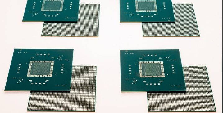
What is FCBGA Substrate?
FCBGA stands for Flip Chip Ball Grid Array, a type of semiconductor package that utilizes flip-chip technology to connect the integrated circuit (IC) to the package substrate. This method involves flipping the silicon die so that its active side faces downward, allowing for direct electrical connections through an array of solder bumps. This configuration contrasts with wire bonding used in traditional packaging methods, offering significant improvements in performance and miniaturization.
Explanation of the Flip-Chip Process and BGA Technology
The flip-chip process in FCBGA involves placing the chip upside down on the substrate, with solder bumps positioned on the chip’s I/O pads. These bumps are then reflowed, creating a reliable electrical connection between the chip and the substrate. This technique enhances signal integrity and reduces the path length for electrical signals, which is crucial for high-frequency applications.
Ball Grid Array (BGA) technology, on the other hand, is a packaging method where the device’s electrical connections are made using a grid of solder balls. These balls serve as the interface between the package and the printed circuit board (PCB). BGA packages are known for their durability and ability to accommodate high pin counts, making them suitable for complex ICs.
Comparison with BGA and Other Packages
While both FCBGA and BGA utilize solder balls for connectivity, the key difference lies in the chip attachment method. In FCBGA, the flip-chip method allows for greater I/O density and improved thermal performance due to the direct contact between the die and the substrate. This is especially beneficial in high-performance computing and telecommunications, where thermal management is critical.
In comparison, FCCSP (Flip Chip Chip Scale Package) is another variant that combines flip-chip technology with chip-scale packaging. FCCSP offers similar advantages in terms of size reduction and performance enhancement but is generally used for applications requiring a smaller form factor than FCBGA. The choice between FCBGA, BGA, and FCCSP depends on the specific requirements of the application, including thermal management, signal integrity, and space constraints.

Get a Quotation For FCBGA Substrate Manufacturer Now
Top FCBGA Substrate Manufacturers
Leading Global Players
The FCBGA (Flip-Chip Ball Grid Array) substrate market is dominated by several global leaders, each known for their advanced manufacturing technologies and ability to supply high-quality substrates for a wide range of applications. Here’s a look at some of the major players in the industry:
ALCANTA
ALCANTA is a prominent player in the semiconductor packaging industry, particularly in the FCBGA substrate segment. Known for its state-of-the-art technology and innovations in materials, ALCANTA specializes in providing high-density substrates with exceptional thermal and electrical performance. Their FCBGA substrates are used extensively in high-performance computing, automotive electronics, and telecommunications. The company focuses on continuously improving its manufacturing processes, incorporating advanced automation and smart manufacturing practices to enhance quality control and efficiency.
TSMC (Taiwan Semiconductor Manufacturing Company)
TSMC, the world’s largest semiconductor foundry, plays a crucial role in the FCBGA substrate market by providing cutting-edge substrate solutions for its semiconductor products. As a key supplier for high-performance chips used in smartphones, AI processors, and high-end computing systems, TSMC integrates FCBGA substrates into its advanced packaging technology. The company’s extensive experience in process control, advanced materials, and manufacturing at scale makes it a leading provider of high-quality FCBGA substrates for global tech giants.
Ibiden
Ibiden is a well-established manufacturer of FCBGA substrates and is known for its advanced, high-density interconnect substrates. With a focus on quality and precision, Ibiden’s substrates are used in high-performance applications, particularly in computing, automotive, and consumer electronics. The company’s R&D initiatives focus on improving the performance and miniaturization of its substrates, integrating newer materials such as organic laminates and innovative manufacturing techniques to meet the growing demands of the semiconductor industry.
Unimicron
Unimicron Technology Corporation, a leading supplier of PCB and FCBGA substrates, has been a major contributor to the global electronics market. The company is recognized for producing high-density substrates that offer excellent signal integrity, thermal management, and electrical performance. Unimicron is particularly strong in providing FCBGA substrates for high-end applications like memory chips, graphics processors, and networking hardware. The company is also at the forefront of adopting sustainable practices, reducing environmental impact by incorporating eco-friendly materials in its manufacturing process.
Shinko Electric
Shinko Electric, a key player in the FCBGA market, has made significant strides in developing advanced packaging solutions, particularly for high-speed computing devices and automotive electronics. With a focus on reliability, Shinko Electric manufactures substrates that offer superior performance under high-stress conditions, such as extreme temperatures and electrical loads. Their commitment to innovation, quality control, and cost-effective production makes them a preferred supplier for top semiconductor companies.
AT&S (Austria Technologie & Systemtechnik)
AT&S is a global leader in the production of high-performance substrates, including FCBGA solutions. The company is well known for its expertise in creating innovative packaging technologies, particularly for applications that require extreme performance, such as 5G, automotive, and industrial electronics. AT&S has invested heavily in its manufacturing capabilities, utilizing advanced equipment and processes to meet the demands of the semiconductor industry. Their dedication to sustainable production and integration of environmentally friendly materials further strengthens their position as a leading supplier of FCBGA substrates.
Key Manufacturers in the Semiconductor Ecosystem
While global giants dominate the FCBGA substrate market, several emerging manufacturers are making significant strides in the industry, particularly in regions with growing semiconductor ecosystems. These companies are leveraging local resources, government initiatives, and the increasing demand for semiconductor components to build a strong foothold in the FCBGA substrate market.
Emerging FCBGA Substrate Suppliers
Several emerging companies are capitalizing on the expanding demand for semiconductor packaging solutions. These suppliers are integrating cutting-edge technologies into their manufacturing processes, focusing on high-density substrates, eco-friendly materials, and advanced designs. Many of these suppliers are forming strategic partnerships with semiconductor manufacturers, ensuring that they stay ahead of the curve in terms of technology and production capabilities. By leveraging the latest advancements in materials science and automation, these companies are able to meet the growing need for FCBGA substrates in applications like AI, data centers, and consumer electronics.
Government Initiatives Supporting Local Manufacturing
Government initiatives play a significant role in fostering the growth of semiconductor packaging industries, including the FCBGA substrate segment. Governments worldwide are recognizing the strategic importance of the semiconductor industry and are offering incentives such as subsidies, tax breaks, and infrastructure support to boost local manufacturing capabilities. These initiatives aim to reduce dependency on foreign suppliers, strengthen local supply chains, and promote the development of advanced manufacturing technologies. The focus is on encouraging both local players and international companies to invest in advanced semiconductor packaging facilities, which includes the production of FCBGA substrates. The increasing support from governments is driving the growth of the FCBGA substrate manufacturing industry, enabling emerging companies to expand their operations and contribute to the global supply of high-performance substrates.

Choosing the Right FCBGA Substrate Manufacturer
Selecting the right FCBGA (Flip-Chip Ball Grid Array) substrate manufacturer is a critical decision for companies in the semiconductor, electronics, and automotive industries. The quality, performance, and reliability of FCBGA substrates are essential for ensuring the success of complex systems such as high-performance processors, GPUs, and telecommunications devices. When choosing a manufacturer, there are several key considerations that can guide the decision-making process.
Key Considerations
Manufacturing Capabilities and Technology Adoption
When evaluating potential FCBGA substrate manufacturers, it’s essential to assess their manufacturing capabilities and the level of technology adoption. Leading manufacturers invest in state-of-the-art equipment and cutting-edge processes to produce high-density, high-performance substrates. These manufacturers often have advanced capabilities in areas like fine-line technology, multi-layer stack-up, and precision etching, which are crucial for producing FCBGA substrates that meet the increasingly complex requirements of modern semiconductor devices. Furthermore, adopting the latest manufacturing technologies like automation, AI-driven quality control, and real-time monitoring ensures greater efficiency and consistency in production.
Manufacturers with strong R&D capabilities and a commitment to technological innovation are often better equipped to meet custom demands and develop next-generation substrates. Look for companies that not only keep up with current trends but are also anticipating future industry needs, such as high-speed interconnects, miniaturization, and packaging solutions for emerging technologies like AI and 5G.
Customization and Scalability Options
Customization is another key factor when selecting a manufacturer for FCBGA substrates. Different applications require unique specifications in terms of size, material composition, electrical performance, and thermal management. A good FCBGA substrate supplier should be able to provide tailored solutions that meet specific design requirements, ensuring that the substrate is optimized for the performance characteristics of the end device.
Scalability is equally important, particularly for companies looking to ramp up production as demand grows. Manufacturers that can scale their production lines to accommodate increasing volumes of substrates while maintaining quality are more valuable partners for long-term projects. Consider manufacturers that offer flexibility in both prototyping and mass production, allowing for a smooth transition from low-volume testing to high-volume production without compromising performance or delivery timelines.
Quality Control and Reliability
Quality control is paramount when selecting an FCBGA substrate manufacturer. The reliability of FCBGA substrates directly impacts the overall performance and longevity of electronic devices. Manufacturers with rigorous testing protocols, such as thermal cycling, stress testing, and electrical performance verification, ensure that substrates can withstand the harsh operating conditions of high-performance applications.
Look for manufacturers that have a strong track record of delivering substrates with minimal defects and high yield rates. Additionally, certifications such as ISO 9001, ISO 14001, and UL (Underwriters Laboratories) approvals can offer additional assurance of the manufacturer’s commitment to quality and regulatory compliance.
Regional Focus: Major FCBGA Manufacturing Hubs
The FCBGA substrate manufacturing landscape is geographically diverse, with several regions emerging as key hubs for semiconductor packaging solutions. Understanding the strengths and focus areas of these regions can help businesses identify the right manufacturer based on location, capabilities, and industry focus.
Taiwan & Japan: Global Leaders in Substrate Technology
Taiwan and Japan have long been dominant players in the semiconductor industry, particularly when it comes to advanced packaging solutions like FCBGA substrates. Companies such as Ibiden, Unimicron, and Shinko Electric are leading the way in FCBGA substrate technology, thanks to their deep expertise in semiconductor packaging and robust manufacturing infrastructure.
- Ibiden: Known for its high-density interconnect substrates, Ibiden is a major player in FCBGA production, offering cutting-edge technology for high-performance applications, including computing, automotive, and telecommunications.
- Unimicron: A key supplier of advanced printed circuit boards (PCBs) and FCBGA substrates, Unimicron provides innovative packaging solutions that enable miniaturization and improve signal integrity for high-speed devices.
- Shinko Electric: Specializing in reliable and high-performance substrates, Shinko Electric’s FCBGA offerings are used in demanding applications, including memory modules, AI processors, and high-end automotive electronics.
These countries are known for their strong R&D environments, highly skilled workforces, and established supply chains, making them reliable sources of FCBGA substrates that meet the most stringent quality and performance standards.
China & South Korea: Rising Powerhouses
China and South Korea have rapidly emerged as rising powerhouses in the semiconductor packaging sector, with significant investments in FCBGA substrate production. China, in particular, has focused on growing its semiconductor manufacturing capabilities through strategic government initiatives and increased private sector investments.
South Korea’s Samsung and SK Hynix have made significant strides in advancing FCBGA packaging for their memory and logic chips. China’s Shaanxi Silverstone, Tongfu Microelectronics, and JCET have also expanded their production capacities to meet the growing demand for advanced packaging technologies.
Both countries benefit from favorable government policies, which have spurred the expansion of FCBGA production. This has created a competitive environment that encourages innovation while driving costs down, making these regions attractive for companies seeking high-quality substrates at scale.
Emerging Semiconductor Packaging Hubs
In addition to Taiwan, Japan, China, and South Korea, there is a growing trend of semiconductor packaging development in regions with emerging economies. These areas are benefiting from government-backed initiatives aimed at strengthening local semiconductor ecosystems, fostering industry growth, and improving competitiveness on the global stage. These hubs are gradually expanding their capabilities to produce advanced substrates such as FCBGA, making them increasingly viable options for sourcing high-quality, cost-effective substrates for a wide variety of industries.
As these regions grow, they will continue to play an important role in the evolution of the FCBGA substrate market, driving technological advancements and offering diverse manufacturing options to meet global demand.
FCBGA vs. Other Packaging Technologies
FCBGA vs. FCCSP
Differences in Design and Application: FCBGA (Flip Chip Ball Grid Array) and FCCSP (Flip Chip Chip Scale Package) are both advanced packaging technologies that utilize flip-chip methods. The primary difference lies in their design and size. FCBGA packages are generally larger, accommodating more I/O pins and providing better heat dissipation, making them suitable for high-performance applications like CPUs and GPUs. In contrast, FCCSP packages are more compact, ideal for mobile and handheld devices where space is at a premium.
Advantages and Disadvantages:
- FCBGA Advantages:
- Higher I/O density and better electrical performance due to the use of C4 bumps.
- Superior thermal management capabilities, crucial for high-power devices.
- FCBGA Disadvantages:
- More complex and expensive to manufacture.
- Larger package size may not be suitable for all applications.
- FCCSP Advantages:
- Smaller form factor, ideal for compact devices like smartphones and tablets.
- Typically lower cost and simpler to assemble compared to FCBGA.
- FCCSP Disadvantages:
- Limited I/O count and thermal performance, restricting use in high-power applications.
Lead Frame vs. Substrate-Based Packages
Comparison of Traditional Lead Frames and Modern Substrate Technologies: Lead frames are a traditional packaging technology where metal leads connect the semiconductor die to the external circuitry. They are commonly used in packages like QFP (Quad Flat Package) and SOP (Small Outline Package). In contrast, substrate-based packages, such as those used in FCBGA, employ a substrate that serves as an interconnect layer, providing a more complex and dense routing path.
Advantages of Substrate-Based Packages:
- Higher Density: Substrates allow for more compact layouts and higher pin counts.
- Improved Performance: Better signal integrity and thermal performance, suitable for high-speed and high-power applications.
- Flexibility: Can support more advanced packaging techniques like flip-chip and multi-chip modules.
Disadvantages of Substrate-Based Packages:
- Cost: Generally more expensive due to the complexity of substrate manufacturing and assembly.
- Design Complexity: Requires more advanced design and fabrication processes.
BGA vs. LFBGA (Low Profile Fine Pitch BGA)
Key Differences and Their Impact on Performance: Both BGA (Ball Grid Array) and LFBGA (Low Profile Fine Pitch BGA) packages utilize an array of solder balls for electrical connections. The primary differences lie in their profile height and pitch (distance between solder balls). LFBGA packages have a lower profile and finer pitch compared to standard BGA, making them suitable for applications where board space is limited.
Impact on Performance:
- LFBGA Advantages:
- Reduced package height, benefiting slim and portable electronic devices.
- Finer pitch allows for higher I/O density in a smaller area.
- LFBGA Disadvantages:
- Increased assembly complexity and potential yield issues due to smaller solder balls.
- More sensitive to thermal and mechanical stresses.
BGA vs. Land Grid Array (LGA)
Structural and Functional Differences: BGA packages use solder balls to connect the package to the PCB, providing both mechanical support and electrical connections. LGA (Land Grid Array) packages, on the other hand, have flat contact pads on the bottom of the package, which mate with corresponding pads on the PCB, typically relying on an external pressure mechanism to ensure a reliable connection.
Functional Implications:
- BGA Advantages:
- Provides a robust mechanical connection that can withstand thermal cycling and mechanical stress.
- Easier to automate in the assembly process.
- BGA Disadvantages:
- Rework and repair are more challenging due to the permanent solder joints.
- LGA Advantages:
- Easier to rework and replace since it does not involve soldering the package to the board.
- Ideal for applications requiring frequent upgrades or changes.
- LGA Disadvantages:
- Requires precise alignment and a secure mounting mechanism to ensure reliable electrical connections.
- Generally offers lower mechanical robustness compared to BGA.
Get a Quotation For FCBGA Substrate Manufacturer Now
Advantages and Disadvantages of FCBGA
Advantages
Higher I/O Density: One of the most significant advantages of FCBGA (Flip Chip Ball Grid Array) packages is their ability to support a high number of input/output (I/O) connections. This is achieved through the use of C4 (Controlled Collapse Chip Connection) bumps, which provide a dense array of electrical connections directly between the semiconductor die and the substrate. This higher I/O density is essential for advanced applications that require fast data transfer and high bandwidth, such as high-performance computing, networking, and graphics processing.
Enhanced Thermal Performance: FCBGA packages are designed to efficiently dissipate heat, a critical feature for high-power devices. The flip-chip design allows for the direct mounting of the die onto the substrate, with the solder bumps facilitating efficient heat transfer from the chip to the substrate and then to a heatsink or other cooling solutions. This enhanced thermal management capability helps maintain the reliability and longevity of the device, preventing thermal degradation and enabling the chip to operate at higher speeds.
Improved Electrical Performance: The reduced distance between the die and the substrate in FCBGA packages minimizes inductance and capacitance, leading to lower signal latency and higher signal integrity. This is particularly beneficial in applications that require precise timing and high-frequency operation, such as RF components and processors.
Compact Design: Despite supporting high I/O counts and enhanced performance features, FCBGA packages can be designed to be relatively compact, saving valuable board space. This makes them suitable for a wide range of applications, including those in compact and portable devices.
Disadvantages
Higher Cost: The complexity of manufacturing FCBGA packages often results in higher costs compared to other packaging technologies. The flip-chip assembly process requires specialized equipment and materials, such as high-precision substrates and high-purity solder bumps. Additionally, the need for stringent quality control measures to ensure reliable solder connections further increases production costs. These factors can make FCBGA an expensive option, particularly for applications where cost is a significant consideration.
Complex Manufacturing Process: The process of assembling FCBGA packages is more complex than traditional packaging methods. It involves precise placement of solder bumps and the die, careful control of the reflow process to ensure proper solder joint formation, and advanced inspection techniques to detect defects. This complexity not only increases manufacturing costs but also poses challenges in terms of yield management and process reliability.
Repair and Rework Challenges: Once soldered onto the PCB, FCBGA packages can be challenging to repair or rework. The dense array of solder bumps and the sensitive nature of the connections make it difficult to desolder and replace the package without damaging the PCB or the component. This can lead to higher repair costs and potentially reduced lifecycle options for products using these packages.
Thermal Expansion Mismatch: The different materials used in FCBGA packages, such as the silicon die, organic substrate, and solder bumps, have different coefficients of thermal expansion (CTE). This mismatch can cause mechanical stress during thermal cycling, potentially leading to solder joint fatigue and failure over time. While advanced design techniques and material selections can mitigate these effects, they do not eliminate the inherent risk.
Get a Quotation For FCBGA Substrate Manufacturer Now
Flip Chip Technology: Beyond FCBGA
Is Flip Chip a BGA?
Flip chip technology is a method used to connect semiconductor devices, but it is not limited to any specific type of package. The term “flip chip” refers to the method of attaching the chip to the substrate, where the chip is flipped so that its active side faces downward, allowing for direct connection through solder bumps. While flip chip technology is commonly used in Ball Grid Array (BGA) packages, such as FCBGA (Flip Chip Ball Grid Array), it is also employed in other package types, including Chip Scale Packages (CSP), Wafer-Level Chip Scale Packages (WLCSP), and even some leaded packages. In essence, flip chip is a versatile interconnection method that enhances electrical and thermal performance, applicable across various packaging technologies.
Explanation of Flip Chip Technology in Various Packages
Flip chip technology improves device performance by shortening the electrical path between the die and the substrate, which reduces inductance and resistance, enhancing signal integrity and speed. The use of solder bumps for electrical connections also provides robust mechanical support and excellent thermal conductivity, making it suitable for high-power and high-frequency applications.
In FCBGA packages, flip chip technology allows for a high density of connections, which is critical for advanced processors and graphics chips. In WLCSP, flip chip technology enables ultra-compact package sizes, essential for mobile and wearable devices. This adaptability makes flip chip technology a cornerstone in modern semiconductor packaging, supporting a wide range of applications from consumer electronics to industrial and automotive systems.
Disadvantages of Flip Chip Technology
Complex Manufacturing Process: One of the main drawbacks of flip chip technology is the complexity involved in its manufacturing process. The precise placement of solder bumps and the need for careful control during the reflow process require sophisticated equipment and strict process control. Any variation in the bump placement or reflow temperature can lead to defects, such as misalignment or voids in the solder joints, affecting the reliability of the package.
Thermal Mismatch: The different materials used in flip chip assemblies, such as silicon for the die, epoxy resins for the substrate, and solder alloys for the bumps, have varying coefficients of thermal expansion (CTE). During temperature changes, these materials expand and contract at different rates, potentially leading to mechanical stress and fatigue in the solder joints. Over time, this can cause cracks and failures, particularly in environments with frequent thermal cycling.
Rework and Repair Challenges: Flip chip packages can be challenging to rework or repair. The dense array of solder bumps makes it difficult to remove the chip without damaging the substrate or surrounding components. Additionally, re-soldering can be problematic due to the risk of damaging the delicate solder joints or altering the alignment of the bumps. This limitation can result in higher repair costs and longer downtime if issues arise after assembly.
Higher Cost: The advanced processes and materials required for flip chip technology contribute to higher manufacturing costs. The need for specialized substrates, high-purity solder materials, and precision equipment increases the overall production expense. For some applications, these costs can be a significant consideration, potentially limiting the use of flip chip technology to high-value or performance-critical products.
Overall, while flip chip technology offers substantial performance benefits, its adoption must consider these challenges and trade-offs. Manufacturers often weigh the performance advantages against the complexity, cost, and reliability considerations when choosing this technology for their products.
Special Considerations in FCBGA Manufacturing
Quality Control and Testing
In the manufacturing of FCBGA (Flip Chip Ball Grid Array) packages, rigorous quality control and testing are crucial to ensure the reliability and performance of the final product. Given the complexity and high density of interconnections in FCBGA packages, even minor defects can lead to significant functional failures.
Importance of Rigorous Testing in Manufacturing:
- Solder Joint Integrity: One of the primary concerns in FCBGA manufacturing is the integrity of the solder joints. Testing methods such as X-ray inspection and automated optical inspection (AOI) are commonly used to detect voids, misalignments, and other defects in the solder bumps. Ensuring strong and reliable solder joints is vital for the mechanical stability and electrical performance of the package.
- Thermal and Mechanical Stress Testing: FCBGA packages are often used in applications with high power and thermal dissipation requirements. Therefore, they undergo thermal cycling and mechanical stress tests to simulate operating conditions. These tests help identify potential issues related to thermal expansion mismatches between different materials, which can lead to solder joint fatigue and failure.
- Electrical Testing: Electrical testing, including continuity tests and functional tests, is conducted to verify the proper operation of the package. This step ensures that all electrical connections are functioning correctly and that the package meets the required performance specifications. In high-frequency applications, signal integrity tests are also crucial to assess the package’s ability to handle high-speed data transfer without degradation.
- Reliability Testing: Long-term reliability tests, such as accelerated aging and environmental testing, are performed to predict the lifespan of the package under various operating conditions. These tests help manufacturers identify potential failure mechanisms and ensure that the product can withstand the intended usage environment.
Innovations and Future Trends
The FCBGA packaging technology continues to evolve, driven by the demands for higher performance, greater miniaturization, and improved energy efficiency. Several emerging technologies and trends are shaping the future of FCBGA manufacturing.
Emerging Technologies and Their Impact on FCBGA Packages:
- Advanced Materials: The development of new materials for substrates and interconnections is a key area of innovation. For example, low-loss dielectric materials and high-conductivity metals are being explored to enhance signal integrity and thermal management. Additionally, the use of materials with better CTE matching can reduce thermal stress and improve the longevity of solder joints.
- Fine Pitch Interconnections: As device performance and integration levels increase, there is a trend towards finer pitch interconnections, allowing for higher I/O densities within the same package footprint. This trend requires advancements in lithography and etching technologies to achieve precise and reliable small-scale features.
- 3D Integration and System-in-Package (SiP) Solutions: The integration of multiple chips within a single package, known as System-in-Package (SiP) technology, is becoming more prevalent. FCBGA packages are increasingly being used in 3D stacked configurations, where multiple dies are stacked vertically and interconnected. This approach enhances performance, reduces latency, and saves space, making it ideal for applications like artificial intelligence, data centers, and high-performance computing.
- Machine Learning and AI in Manufacturing: The use of machine learning and artificial intelligence in the manufacturing process is becoming more common. These technologies can optimize production parameters, predict potential defects, and enhance quality control. By analyzing large datasets from the manufacturing process, AI can help identify patterns and correlations that human operators might miss, leading to improvements in yield and product reliability.
- Green Manufacturing Practices: As environmental concerns grow, there is increasing emphasis on sustainable manufacturing practices. This includes the development of eco-friendly materials, reducing waste and energy consumption, and ensuring that FCBGA packages are designed for recyclability. Green manufacturing practices not only benefit the environment but can also reduce costs and improve the company’s reputation.
Overall, these innovations and trends are pushing the boundaries of what is possible with FCBGA technology, enabling the development of faster, smaller, and more efficient electronic devices. As these technologies mature, they will continue to play a crucial role in meeting the demands of next-generation electronic applications.
Get a Quotation For FCBGA Substrate Manufacturer Now
Contact Us NOW
FAQs About FCBGA Substrate Manufacturer
What is the difference between FCBGA and BGA?
FCBGA (Flip Chip Ball Grid Array) and BGA (Ball Grid Array) both use an array of solder balls for connections between the semiconductor die and the PCB. The key difference is in the chip attachment method. FCBGA uses flip-chip technology, where the die is flipped so that its active side faces the substrate, allowing for direct solder connections via C4 bumps. In contrast, standard BGA packages may use wire bonding or other methods for die attachment. FCBGA generally offers better electrical performance and thermal management due to the direct connection and smaller distance between the die and the substrate.
What does FCBGA stand for?
FCBGA stands for Flip Chip Ball Grid Array.
What is the FCBGA package?
An FCBGA package is a type of semiconductor package that utilizes flip-chip technology and a ball grid array configuration. In this package, the semiconductor die is flipped so that the active side is facing down, and the electrical connections are made through solder bumps (C4 bumps) directly to the substrate. This design allows for a higher density of connections, improved thermal performance, and better electrical signal integrity compared to traditional packaging methods.
What is the substrate material for flip chip?
The substrate material for flip-chip packages, including FCBGA, is typically an organic material like glass-reinforced epoxy resin (FR-4) or more advanced materials such as BT (Bismaleimide-Triazine) resin or PI (Polyimide). For high-performance applications, advanced ceramics or polyimide-based materials may be used to provide better thermal and electrical properties.
What are the disadvantages of BGA?
BGA disadvantages include:Rework Challenges: Once the BGA is soldered onto the PCB, it is difficult to rework or replace the package without causing damage to the PCB or other components.
Thermal Management: While BGAs offer good thermal performance, the heat dissipation can be limited if not properly managed.
Inspection Difficulties: The solder joints are hidden under the package, making visual inspection and fault detection challenging. This requires X-ray or other advanced inspection methods.
Is flip chip a BGA?
Flip chip is not a specific type of BGA, but it is a technology used within BGA packages. In a flip-chip BGA (FCBGA), the flip-chip process is used to connect the die to the substrate via solder bumps, while the BGA configuration refers to the array of solder balls used for mounting the package on the PCB.
What are the disadvantages of flip chip?
Thermal Mismatch: Different materials used in the package can lead to thermal expansion mismatch, causing mechanical stress and potential solder joint failure.
Repair Challenges: The dense array of solder bumps makes it difficult to repair or rework flip-chip packages.
What does C4 bump stand for?
C4 bump stands for Controlled Collapse Chip Connection. It refers to the solder bumps used in flip-chip technology to create electrical connections between the semiconductor die and the substrate.
What is the main advantage of a flip chip package?
The main advantage of a flip-chip package is its improved electrical performance and thermal management. The direct connection of the die to the substrate through C4 bumps reduces electrical path lengths and signal integrity issues, while the flip-chip design enhances heat dissipation compared to other packaging methods.
What is the difference between BGA and LFBGA?
BGA (Ball Grid Array) and LFBGA (Low Profile Fine Pitch BGA) are both types of ball grid array packages. The key differences are:Profile Height: LFBGA packages have a lower profile height compared to standard BGA packages, making them suitable for applications where space is constrained.
Pitch Size: LFBGA features a finer pitch (smaller distance between solder balls) than standard BGA, allowing for higher I/O density in a smaller footprint.
What is the difference between BGA and Land Grid Array (LGA)?
BGA (Ball Grid Array) uses solder balls arranged in a grid pattern for connections, which provide both electrical connectivity and mechanical support. Land Grid Array (LGA), on the other hand, uses flat pads on the package that make contact with corresponding pads on the PCB. The main differences are:Connection Method: BGA relies on solder balls for electrical connections, while LGA uses pressure contact.
Rework and Repair: LGA packages are generally easier to rework or replace compared to BGA packages, which require desoldering.
What is the difference between green algae and BGA?
Green algae and BGA (Ball Grid Array) are unrelated concepts. Green algae refers to a group of photosynthetic organisms found in aquatic environments, while BGA is a type of semiconductor package used in electronics. The term “BGA” pertains to technology and packaging, whereas “green algae” pertains to biology and ecology.
What is the difference between BGA and FPGA?
BGA (Ball Grid Array) is a packaging technology used for semiconductor devices, including integrated circuits. FPGA (Field-Programmable Gate Array), on the other hand, is a type of semiconductor device that can be programmed to perform various logic functions after manufacturing. The differences are:Function: BGA is a package type, while FPGA is a type of chip.
Application: BGA packages can house various types of chips, including FPGAs, but FPGAs are specific types of programmable logic devices used for custom digital circuits.

