
Understanding Direct Bonded Copper Substrate Benefits
Direct bonded copper substrate (DBC) substrates are integral components in semiconductor technology, offering crucial benefits in thermal management and electrical connectivity. These substrates provide a robust foundation for semiconductor devices, ensuring efficient heat dissipation and reliable performance. Through a specialized manufacturing process, direct bonding technology enables the seamless integration of copper layers onto ceramic substrates, enhancing thermal conductivity and mechanical stability. Direct bonded copper substrate finds extensive applications in power electronics, automotive systems, and renewable energy devices, where high power densities and thermal demands necessitate superior material properties. Understanding the intricacies of direct bonded copper substrate is paramount for optimizing device performance and ensuring longevity in challenging operating conditions.
What is a Substrate in Semiconductor Technology? Understanding the Role of Direct Bonded Copper Substrate
Definition and Role of Substrates in Semiconductor Devices
In semiconductor technology, substrates serve as the fundamental platform upon which semiconductor components are constructed and integrated. These substrates provide essential structural support and facilitate the interconnection of various components within semiconductor devices. Typically composed of materials like silicon, ceramic, or metal, substrates are chosen for their specific properties and compatibility with the intended application.
Importance of Substrates for Providing Structural Support, Thermal Management, and Electrical Connectivity
Structural Support: Substrates are crucial for ensuring the mechanical integrity and stability of semiconductor devices. They offer a solid foundation for mounting and securing individual components such as integrated circuits (ICs), transistors, and diodes, safeguarding against deformation or damage during operation and handling.
Thermal Management: Efficient heat dissipation is paramount for the reliable performance of semiconductor devices, particularly those with high power densities. Substrates with exceptional thermal conductivity, like direct bonded copper substrates, facilitate the dissipation of heat generated during operation, preventing overheating and thermal-induced failures. By effectively transferring heat away from sensitive components, substrates contribute to the longevity and reliability of semiconductor devices.
Electrical Connectivity: Substrates play a pivotal role in establishing electrical connectivity between different components within semiconductor devices, enabling the flow of electrical signals and power. Through the integration of conductive traces, vias, and bonding pads, substrates create the necessary electrical pathways for interconnecting ICs, linking to external circuits, and implementing various functionalities within the device.
Direct Bonded Copper Substrate in Semiconductor Technology: Direct bonded copper substrates epitomize the significance of substrates in semiconductor technology. These substrates are meticulously engineered to provide superior thermal conductivity and mechanical stability, making them well-suited for applications requiring efficient thermal management and high reliability. By seamlessly integrating copper layers onto ceramic substrates through advanced bonding techniques, direct bonded copper substrates enhance the performance and durability of semiconductor devices operating under demanding thermal conditions.
Types of Substrates: Understanding Direct Bonded Copper Substrate and Other Variants in Semiconductor Technology
Overview of Various Substrate Types Used in Semiconductor Technology
In semiconductor technology, a diverse range of substrate types caters to the varied needs of different applications. These substrates vary in material composition, fabrication methods, and performance characteristics. Among them, Direct Bonded Copper (DBC) substrate stands out for its remarkable thermal conductivity and mechanical robustness, making it an optimal choice for applications demanding efficient thermal management and high reliability.
Direct Copper Bonding (DCB) Substrate: DCB substrates are crafted by directly bonding copper layers onto ceramic substrates using advanced bonding methodologies. This process yields substrates with outstanding thermal conductivity and mechanical resilience, rendering them well-suited for power electronics, automotive systems, and other high-power applications. DCB substrates surpass traditional substrates in thermal performance, facilitating effective heat dissipation and augmenting device reliability.
Active Metal Brazed (AMB) Substrate: AMB substrates are fabricated by brazing metal layers onto ceramic or metal substrates employing active metal brazing techniques. These substrates offer commendable thermal conductivity and mechanical stability, making them appropriate for applications necessitating moderate thermal management capabilities. AMB substrates find utility in diverse industries, including aerospace, telecommunications, and medical devices.
Insulated Metal Substrate (IMS): IMS substrates feature a metal core ensconced between insulating layers, typically composed of ceramics or polymers. These substrates strike a balance between thermal performance and electrical insulation, rendering them suitable for applications wherein both factors are pivotal, such as LED lighting, power modules, and motor drives. IMS substrates facilitate efficient heat dissipation while preserving electrical isolation between components.
Others: Apart from the aforementioned substrates, there exist other types utilized in semiconductor technology, encompassing:
- Silicon substrates: Prevalently employed in integrated circuits (ICs) and microelectromechanical systems (MEMS).
- Organic substrates: Deployed in flexible electronics and printed circuit boards (PCBs).
- Glass substrates: Utilized in displays, sensors, and optical devices.
Each substrate type offers distinct advantages and is chosen based on the specific requisites of the application. Nevertheless, DBC substrates, distinguished by their superior thermal conductivity and mechanical durability, continue to be favored for demanding applications in semiconductor technology.
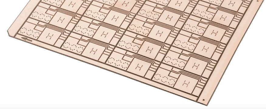
Understanding Direct Bonded Copper (DBC) Substrates: Unveiling the Intricacies of Direct Bonded Copper Substrate
Direct Bonded Copper (DBC) substrates represent a sophisticated solution in semiconductor technology, characterized by their exceptional thermal conductivity, mechanical strength, and reliability. Let’s delve deeper into the details of DBC substrates:
Definition and Composition: Direct Bonded Copper substrates are engineered structures comprising a ceramic base material, typically alumina (Al2O3), onto which copper layers are directly bonded. This bonding process creates a robust interface between the copper and ceramic layers, ensuring efficient thermal conduction and mechanical stability.
Manufacturing Process: The manufacturing of DBC substrates involves several intricate steps. Initially, ceramic substrates are prepared by shaping and sintering alumina powder into precise dimensions. Subsequently, copper foils are meticulously cleaned and bonded to the ceramic substrate under controlled conditions using advanced bonding techniques such as high temperature and pressure. This process results in a seamless integration of copper layers onto the ceramic base, forming the DBC substrate.
Properties and Advantages
- Excellent Thermal Conductivity: DBC substrates exhibit outstanding thermal conductivity due to the direct bonding of copper, which efficiently dissipates heat away from semiconductor components. This property is crucial for managing thermal loads in high-power electronic devices.
- High Mechanical Strength: The direct bonding process ensures strong adhesion between the copper and ceramic layers, enhancing the mechanical strength of DBC substrates. This enables them to withstand mechanical stresses and environmental conditions encountered during device operation and handling.
- Low Thermal Expansion Coefficient: DBC substrates possess a low thermal expansion coefficient, meaning they experience minimal dimensional changes with temperature fluctuations. This characteristic reduces the risk of thermal mismatch-induced stresses, which can lead to device failure over time.
- Enhanced Reliability: DBC substrates offer enhanced reliability compared to conventional substrates. Their robust construction and excellent thermal management capabilities contribute to prolonged device lifetimes and reduced failure rates, making them a preferred choice for mission-critical applications.
Direct Bonded Copper substrates combine superior thermal conductivity, mechanical strength, and reliability, making them indispensable components in various semiconductor devices, especially those operating under high-power and high-temperature conditions.
Direct Copper Bonding Technology: Exploring the Intricacies of the DBC Fabrication Process
Direct Copper Bonding (DCB) technology lies at the heart of creating Direct Bonded Copper substrates, offering a precise and efficient method for integrating copper layers onto ceramic substrates. Let’s delve into the details of the DCB fabrication process:
Steps Involved in DBC Fabrication
- Surface Preparation: The process begins with the meticulous cleaning and preparation of both the ceramic substrate and the copper foils. Any contaminants or impurities on the surfaces must be removed to ensure optimal bonding.
- Alignment and Bonding: The prepared copper foils are aligned and placed onto the ceramic substrate with precision. High temperature and pressure are applied to initiate the bonding process, allowing the copper to metallurgically bond with the ceramic surface. This step is crucial for achieving a strong and durable bond between the layers.
- Thermal Treatment: After bonding, the assembled substrate undergoes thermal treatment to further enhance the adhesion between the copper and ceramic layers. This step helps alleviate residual stresses and improves the overall stability of the substrate.
- Post-Bonding Processing: Following thermal treatment, the bonded substrate may undergo additional processing steps such as machining, surface finishing, and quality inspection to ensure adherence to specifications and standards.
Key Technologies and Equipment Used
- Precision Alignment Systems: Advanced alignment systems are employed to ensure accurate placement of copper foils onto ceramic substrates, minimizing misalignment and enhancing bond quality.
- High-Temperature Furnaces: Specialized furnaces capable of reaching elevated temperatures are utilized for the bonding process. These furnaces provide the controlled thermal environment necessary for achieving proper bonding between the copper and ceramic layers.
- Pressure Application Systems: Hydraulic or pneumatic pressure systems are employed to apply uniform pressure during the bonding process. Consistent pressure distribution is essential for promoting intimate contact between the bonding surfaces and facilitating metallurgical bonding.
Importance of Precise Control and Quality Assurance
Precision control and quality assurance are paramount throughout the DBC fabrication process to ensure the reliability and performance of the resulting substrates. Any deviation from the specified parameters or defects in the bonding process can compromise the integrity of the substrate and affect its thermal and mechanical properties. Therefore, stringent quality control measures, including thorough inspections, material testing, and process monitoring, are implemented to maintain consistency and reliability in DBC substrate production. By adhering to strict quality standards, manufacturers can deliver substrates that meet the rigorous demands of semiconductor applications, contributing to the success and longevity of electronic devices.
Active Metal Brazed (AMB) Substrates: Exploring an Alternative to DBC
Introduction to AMB Substrates
Active Metal Brazed (AMB) substrates offer an alternative approach to achieving reliable thermal management and electrical connectivity in semiconductor devices. Unlike Direct Bonded Copper (DBC) substrates, AMB substrates are fabricated by brazing metal layers onto ceramic or metal substrates using active metal brazing techniques.
Definition and Composition
AMB substrates consist of multiple layers of metal, typically copper or aluminum, bonded to a ceramic or metal base material. The bonding process involves the use of active metals, such as titanium or zirconium, which form intermetallic compounds with the substrate and the metal layers, facilitating strong adhesion.
Contrasting Features with DBC Substrates
While both AMB and DBC substrates aim to provide effective thermal management and electrical connectivity, they differ in their fabrication methods and material properties:
- Fabrication Method: DBC substrates are formed through a direct bonding process, where copper layers are directly bonded to ceramic substrates. In contrast, AMB substrates utilize brazing techniques to attach metal layers onto substrates, allowing for greater flexibility in material selection and design.
- Material Properties: DBC substrates are renowned for their excellent thermal conductivity and mechanical strength, owing to the direct bonding of copper layers. On the other hand, AMB substrates may offer different material properties depending on the choice of metals and brazing materials used. While they may exhibit good thermal conductivity, they may not match the thermal performance of DBC substrates in all cases.
Applications and Suitability
AMB substrates find applications in various industries and technologies, including:
- Aerospace and Defense: AMB substrates are utilized in electronic modules and components for aerospace and defense applications, where reliability and performance under extreme conditions are critical.
- Telecommunications: AMB substrates are suitable for telecommunications equipment, providing efficient thermal management and electrical connectivity in high-frequency and high-power devices.
- Medical Devices: AMB substrates are used in medical devices such as imaging equipment and patient monitoring systems, where compact size, reliability, and thermal performance are essential.
While AMB substrates offer advantages in certain applications, such as flexibility in material selection and design, they may not always match the thermal performance and reliability of DBC substrates. Therefore, the choice between AMB and DBC substrates depends on the specific requirements and constraints of the application at hand.
Comparing DBC and AMB Substrates: A Comprehensive Analysis
When evaluating substrates for semiconductor applications, comparing Direct Bonded Copper (DBC) and Active Metal Brazed (AMB) substrates is essential. Let’s delve into a detailed comparative analysis:
Thermal Performance:
- DBC Substrates: DBC substrates are renowned for their exceptional thermal conductivity, owing to the direct bonding of copper layers onto ceramic substrates. This enables efficient heat dissipation, making them ideal for high-power applications where thermal management is critical.
- AMB Substrates: AMB substrates also offer good thermal conductivity, depending on the choice of metals and brazing materials used. While they may not match the thermal performance of DBC substrates in all cases, AMB substrates can still provide effective heat dissipation in many applications.
Mechanical Properties:
- DBC Substrates: DBC substrates exhibit high mechanical strength due to the strong bond between the copper and ceramic layers. This makes them resistant to mechanical stresses and environmental factors, ensuring long-term reliability.
- AMB Substrates: AMB substrates may vary in mechanical properties depending on the choice of materials and brazing techniques. While they can provide adequate mechanical strength, the properties may not be as consistent as those of DBC substrates.
Cost-effectiveness:
- DBC Substrates: DBC substrates may have higher initial manufacturing costs due to the complexity of the direct bonding process. However, their excellent thermal performance and reliability can lead to cost savings in the long run by reducing the need for additional thermal management solutions and minimizing device failures.
- AMB Substrates: AMB substrates may offer cost advantages in certain cases, especially for low- to medium-power applications where the requirements for thermal performance and reliability are less stringent. The flexibility in material selection and the brazing process may also contribute to cost-effectiveness.
Application-specific Considerations:
- DBC Substrates: DBC substrates are well-suited for high-power applications in industries such as automotive, power electronics, and renewable energy, where efficient thermal management and reliability are paramount.
- AMB Substrates: AMB substrates find applications in a wide range of industries, including aerospace, telecommunications, and medical devices, where specific material properties and design flexibility are required. They may be preferred for applications where cost constraints outweigh the need for the highest thermal performance.
The choice between DBC and AMB substrates depends on the specific requirements of the application, including thermal performance, mechanical properties, cost considerations, and application-specific factors. While DBC substrates excel in thermal conductivity and reliability, AMB substrates offer flexibility and cost advantages in certain scenarios.
Applications of DBC Substrates: Unleashing the Potential Across Various Industries
Direct Bonded Copper (DBC) substrates find extensive applications across diverse industries, leveraging their superior thermal conductivity, mechanical strength, and reliability. Let’s explore some key sectors benefiting from the utilization of DBC substrates:
Power Electronics: In the realm of power electronics, DBC substrates play a pivotal role in devices such as insulated gate bipolar transistors (IGBTs), diode modules, and thyristors. Their exceptional thermal conductivity enables efficient heat dissipation, allowing these devices to handle high-power densities while maintaining optimal operating temperatures. DBC substrates are integral components in power converters, inverters, motor drives, and other power electronic systems, enhancing performance and reliability.
Automotive Industry: The automotive sector relies on DBC substrates for various applications, including electric vehicle (EV) powertrains, battery management systems (BMS), and onboard charging systems. DBC substrates facilitate the efficient thermal management of power electronics in EVs, ensuring optimal performance and longevity of battery packs and electric drivetrains. Additionally, they are utilized in automotive lighting systems, engine control modules (ECMs), and hybrid electric vehicle (HEV) power converters, contributing to improved efficiency and safety in vehicles.
Renewable Energy Systems: In renewable energy systems such as solar inverters, wind turbines, and energy storage systems, DBC substrates play a critical role in enhancing efficiency and reliability. By effectively dissipating heat generated during power conversion processes, DBC substrates enable renewable energy systems to operate at peak performance levels while minimizing energy losses. They are also utilized in grid-tied inverters, microinverters, and power optimizers, supporting the integration of renewable energy sources into the electrical grid.
Aerospace and Defense: The aerospace and defense industries leverage DBC substrates in a wide range of applications, including avionics, radar systems, communication devices, and electronic warfare systems. DBC substrates offer superior thermal management capabilities, making them well-suited for harsh operating environments encountered in aerospace and defense applications. They contribute to the reliability and performance of electronic systems deployed in aircraft, satellites, unmanned aerial vehicles (UAVs), and military vehicles, ensuring mission success and safety.
Others: Beyond the aforementioned sectors, DBC substrates find applications in various other industries, including telecommunications, industrial automation, medical devices, and consumer electronics. They are utilized in high-power RF amplifiers, laser diode drivers, LED lighting systems, and power supplies, among others, where efficient thermal management and reliability are paramount.
DBC substrates serve as indispensable components across a multitude of industries, enabling the development of high-performance electronic systems with enhanced thermal management capabilities and reliability. Their versatility and superior properties make them invaluable assets in driving innovation and progress across diverse technological domains.
Industry Spotlight: Rogers Corporation: Leading the Way in Advanced Materials and Semiconductor Technology
Brief Overview of Rogers Corporation: Rogers Corporation stands as a global leader in the development and manufacturing of advanced materials that enable cutting-edge technologies across various industries. With a rich history dating back to 1832, Rogers has continually evolved to meet the evolving needs of modern industries, leveraging expertise in materials science, engineering, and innovation.
Rogers Corporation’s portfolio encompasses a diverse range of materials, including high-performance polymers, elastomers, foam, and ceramics. Among its flagship products are Direct Bonded Copper (DBC) substrates, which have garnered widespread recognition for their exceptional thermal management capabilities and reliability in semiconductor applications.
Contribution to Semiconductor Technology and Innovation: Rogers Corporation’s contributions to semiconductor technology and innovation are significant and far-reaching. Through its development of DBC substrates, Rogers has revolutionized thermal management solutions in high-power electronic devices, such as power modules, RF amplifiers, and LED lighting systems.
The company’s DBC substrates offer unparalleled thermal conductivity, mechanical strength, and reliability, addressing critical challenges faced by semiconductor manufacturers in optimizing device performance and longevity. By providing a reliable platform for integrating power semiconductor components, Rogers has facilitated advancements in power electronics, automotive electronics, renewable energy systems, and aerospace applications.
Moreover, Rogers Corporation’s commitment to research and development ensures ongoing advancements in material science and engineering, driving continuous improvement and innovation in semiconductor technology. Collaborations with industry partners and academic institutions further enhance Rogers’ capabilities to develop next-generation materials and solutions that meet the evolving demands of the semiconductor industry.
Rogers Corporation’s leadership in advanced materials, exemplified by its DBC substrates, continues to shape the landscape of semiconductor technology, enabling the development of high-performance electronic devices that power modern society and drive innovation across industries.
FAQs About Direct Bonded Copper Substrate
Direct Bonded Copper (DBC) substrate is a type of substrate used in semiconductor technology. It involves directly bonding copper layers onto ceramic substrates using advanced bonding techniques. DBC substrates offer excellent thermal conductivity, mechanical strength, and reliability, making them ideal for applications requiring efficient thermal management.
The difference between DBC and AMB substrates lies in their fabrication methods and material properties. DBC substrates are formed by directly bonding copper layers onto ceramic substrates, whereas AMB substrates are created by brazing metal layers onto ceramic or metal substrates using active metal brazing techniques. While both substrates aim to provide effective thermal management and electrical connectivity, DBC substrates typically offer higher thermal conductivity and mechanical strength compared to AMB substrates.
DCB substrate is a common typo or misspelling for DBC substrate. They both refer to Direct Bonded Copper substrates.
In summary, DBC (Direct Bonded Copper) substrates involve directly bonding copper layers onto ceramic substrates, providing excellent thermal conductivity and mechanical strength. AMB (Active Metal Brazed) substrates, on the other hand, are created by brazing metal layers onto substrates using active metal brazing techniques, offering different material properties compared to DBC substrates.

