
Benefits of Custom FCBGA Package Substrate Service
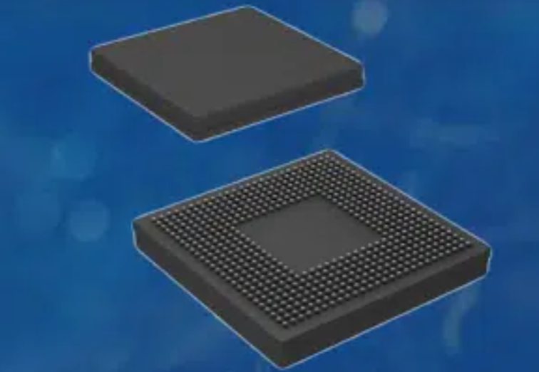
FCBGA (Flip-Chip Ball Grid Array) is an advanced semiconductor packaging technology where the chip is flipped upside down and soldered directly onto a substrate with an array of solder balls, allowing for efficient electrical connections and superior thermal management. This packaging technology plays a vital role in modern electronics by enabling high-density interconnections, smaller form factors, and improved performance. FCBGA is essential in industries such as telecommunications, automotive, and consumer electronics, where there is a constant demand for faster, more reliable, and power-efficient devices. With these requirements in mind, Custom FCBGA Package Substrate Service has become crucial in tailoring substrates to meet specific performance, size, and thermal needs, supporting a broad range of applications.
Importance of Custom FCBGA Package Substrate Service
Substrates play a critical role in flip-chip packaging, acting as the foundation that supports the chip and facilitates its electrical and thermal functions. In flip-chip technology, the substrate connects the chip to the external world through solder balls, which form the electrical pathways. The substrate also provides the necessary mechanical stability to ensure reliable chip performance under various environmental conditions. Moreover, substrates are responsible for efficient heat dissipation, ensuring that the chip remains within optimal temperature ranges, thus preventing overheating and ensuring long-term reliability.
When it comes to Custom FCBGA Package Substrate Service, the ability to tailor substrates to meet specific needs is one of the key advantages. Customization allows substrates to be designed with particular specifications such as size, thickness, and material, which can significantly enhance performance. For example, using specialized materials can improve signal integrity and minimize power loss, while custom thicknesses can be chosen for better thermal management and heat dissipation.
The process of customizing FCBGA substrates also brings cost-effective advantages. By precisely meeting the requirements of the application, manufacturers can reduce waste, lower production costs, and improve yield. Furthermore, a custom approach accelerates time-to-market by streamlining the design and prototyping phases. Custom FCBGA Package Substrate Service ensures that the final product is not only optimized for performance but also for cost-efficiency, providing significant value to businesses in competitive industries.
Key Features of Custom FCBGA Package Substrates in Custom FCBGA Package Substrate Service
Custom FCBGA Package Substrate Service offers several key features that make it an essential component in the world of advanced semiconductor packaging. These features include the materials used in the substrates, design flexibility, and the crucial thermal and electrical properties that influence overall performance.
Materials Used in FCBGA Substrates
The materials selected for FCBGA substrates are critical to achieving the desired performance characteristics. Common materials include organic laminates, ceramics, and other high-performance materials. Organic laminates are often used due to their cost-effectiveness and ease of manufacturing, while ceramics provide superior thermal and electrical performance for high-power applications. Other specialized materials may be selected based on specific needs, such as high-speed signal processing or demanding thermal management requirements. For example, in applications requiring high-speed signals, materials with low dielectric constants are chosen to minimize signal loss and maintain signal integrity. The selection of the right material is essential for meeting the specific requirements of each application, which is why Custom FCBGA Package Substrate Service allows for precise material customization to fit these needs.
Design Flexibility
One of the standout features of Custom FCBGA Package Substrate Service is the design flexibility it offers. Substrates can be customized in terms of layer count, via structures, and size to meet the exact requirements of each product. The number of layers in a substrate influences its ability to handle more complex signal routing, while via structures, including microvias or blind vias, enable higher-density interconnections that support advanced semiconductor functionality. Customization of substrate size is also essential for ensuring that it fits within the space constraints of the final device. Precision in these design elements is paramount for high-performance devices, ensuring that the substrate can handle the electrical, mechanical, and thermal demands of modern electronics.
Thermal and Electrical Properties
Thermal and electrical properties are crucial in ensuring that the custom substrate delivers optimal performance. Heat management is a primary concern in flip-chip packaging, especially for high-power devices. Custom substrates are often designed with materials like copper and thermal vias to enhance heat dissipation and prevent overheating. Copper is commonly used for its excellent thermal conductivity, ensuring that heat generated by the chip is efficiently transferred away from sensitive components. Thermal vias help direct heat away from the chip and spread it throughout the substrate, enhancing the thermal stability of the device.
On the electrical side, the primary focus is on minimizing signal loss and enhancing high-frequency performance. Custom FCBGA Package Substrate Service ensures that substrates are designed with optimal electrical characteristics, such as low resistance and low inductance, to ensure high-speed signal transmission without degradation. The precision of the vias and the material selection further improve signal integrity, which is critical in applications such as telecommunications, computing, and consumer electronics, where high-frequency signals need to be transmitted with minimal interference.
By combining these advanced material choices, design flexibility, and superior thermal and electrical properties, Custom FCBGA Package Substrate Service allows for the creation of substrates tailored to meet the most demanding performance requirements, ensuring that devices operate efficiently and reliably in a variety of industries.
Steps in Custom FCBGA Package Substrate Service Manufacturing
The manufacturing process of Custom FCBGA Package Substrate Service typically begins with the Design Phase, where the primary focus is on collaborating closely with customers to understand their specific technical requirements and constraints. This includes analyzing the application’s performance needs, such as signal integrity, thermal management, and physical dimensions. By gathering detailed information, engineers can design substrates that meet these precise requirements. During this phase, simulation and modeling play a vital role in optimizing the substrate design, ensuring that all aspects of the package, from the layer structure to the via placement, align with the customer’s needs and industry standards.
Once the design is finalized, the next step is Prototyping and Testing. In this phase, prototypes are created to verify the design under real-world conditions. The prototypes undergo rigorous testing for electrical and thermal properties, ensuring that the final product will perform as expected. Electrical tests verify signal integrity, while thermal testing ensures that the substrate can effectively dissipate heat, preventing potential overheating issues. This step is essential to identify any potential issues early in the process, allowing for design tweaks before moving to large-scale production.
The final stage is Mass Production, where the prototype moves into full-scale production. At this stage, the transition from prototype to mass production must be carefully managed to maintain the integrity of the design. Manufacturers implement stringent quality control measures throughout the production process, ensuring that every substrate meets the required standards. Reliability testing is also conducted to ensure that the custom FCBGA substrates can withstand long-term use and operate effectively in their intended environments. Through these steps, Custom FCBGA Package Substrate Service ensures that the final product is of the highest quality and reliability, tailored to meet the specific needs of the customer.
Leading Companies Offering Custom FCBGA Package Substrate Service
Several major companies offer Custom FCBGA Package Substrate Service, each bringing unique capabilities to the table. These companies provide a range of customizable solutions for different industries, ensuring that businesses can find the right substrate for their specific needs. Some of the most well-known providers in this field include Venture MFG, Alcanta PCB, Toppan, Amkor, Shinko, ASE, and QP Technologies.
Overview of Major Providers
-
Venture MFG: Specializing in high-quality custom substrates, Venture MFG offers tailored FCBGA packaging solutions with a strong emphasis on quick turnaround times and customer collaboration. Their services are widely used across various industries, including telecommunications and consumer electronics.
-
Alcanta PCB: Known for providing robust PCB and FCBGA substrate services, Alcanta PCB focuses on high-performance solutions for demanding applications. Their customization options include a wide selection of materials and designs, making them a popular choice for customers requiring precise, high-density interconnects.
-
Toppan: A global leader in electronic packaging, Toppan offers advanced Custom FCBGA Package Substrate Service with cutting-edge technologies. Their substrates are commonly used in high-performance computing, automotive, and telecommunications industries, where signal integrity and heat management are crucial.
-
Amkor: With decades of experience in semiconductor packaging, Amkor provides a broad range of packaging services, including custom FCBGA substrates. Their solutions cater to industries like mobile devices, automotive, and consumer electronics, where reliability and miniaturization are essential.
-
Shinko: Shinko specializes in high-quality packaging and custom substrates, particularly in the field of electronics. Their FCBGA solutions focus on achieving the highest performance in terms of signal integrity and thermal management, serving industries such as automotive and industrial applications.
-
ASE: ASE is a major player in semiconductor packaging, offering Custom FCBGA Package Substrate Service with a focus on cutting-edge technologies and efficient production processes. ASE serves industries including telecommunications, computing, and consumer electronics, with an emphasis on custom designs and high-reliability solutions.
-
QP Technologies: QP Technologies is known for its innovative approach to FCBGA substrate manufacturing, offering tailored solutions for customers in markets such as telecommunications, aerospace, and industrial automation. Their expertise in high-frequency applications sets them apart in the field.
Comparing Their Services
While all of these companies offer Custom FCBGA Package Substrate Service, their capabilities vary in terms of the level of customization and technological features they provide:
-
Customization Options: Companies like Alcanta PCB and QP Technologies provide highly specialized designs, offering flexibility in layer count, via structure, and materials. Meanwhile, larger providers like Amkor and ASE offer more standardized solutions but can handle larger-scale orders with faster lead times.
-
Technological Capabilities: Toppan and Shinko are at the forefront of utilizing advanced materials and high-density interconnects, offering solutions for industries requiring cutting-edge performance. On the other hand, companies like Venture MFG may focus on providing quicker, cost-effective solutions for smaller-scale applications without compromising on quality.
-
Industries Served: The major industries served by these providers include telecommunications, consumer electronics, automotive, aerospace, and high-performance computing. For example, Amkor is widely known for its presence in the mobile phone industry, while ASE and Toppan cater heavily to automotive and telecommunications sectors.
Choosing the Right Provider
When selecting a provider for Custom FCBGA Package Substrate Service, several factors should be taken into account:
-
Lead Time: Depending on the urgency of your project, you may need a provider who can deliver a faster turnaround time. Venture MFG and Alcanta PCB are known for their shorter lead times, making them ideal for customers needing rapid prototyping and quick deliveries.
-
Quality Certifications: Ensure that the provider holds the necessary industry certifications such as ISO 9001, TS16949, or other relevant certifications to guarantee product quality and consistency. ASE, Toppan, and Amkor, for example, maintain rigorous quality control standards for their manufacturing processes.
-
Cost: Custom FCBGA substrates can vary in price depending on factors such as material choice, complexity of design, and volume. Smaller providers like Venture MFG may offer more cost-effective solutions, while larger companies like ASE and Amkor may offer competitive pricing for bulk orders.
-
Customer Support: Reliable customer support is critical, especially during the design and prototyping phases. Choosing a provider with strong customer service can make a significant difference in ensuring the success of your custom substrate project. QP Technologies and Alcanta PCB are noted for their customer-centric approaches and close collaboration with clients.
By considering these factors, businesses can choose the most suitable provider for their Custom FCBGA Package Substrate Service needs, ensuring optimal performance, cost-efficiency, and timely delivery for their specific application.
Benefits of Using Custom FCBGA Package Substrate Service in Electronic Products
Custom FCBGA Package Substrate Service provides a range of significant benefits, including improved performance, enhanced customization for advanced electronics, and cost-effectiveness in long-term production. These advantages make custom substrates a vital component in the development of high-performance electronic products.
Improved Performance
One of the primary benefits of using custom FCBGA substrates is the enhanced signal integrity they provide. In electronic devices, especially those requiring high-speed signal transmission, signal loss and interference can lead to reduced performance. By customizing the substrate with materials that have low dielectric constants, designers can minimize signal degradation, ensuring clearer and faster data transmission. Additionally, custom substrates can be engineered to reduce power consumption, an essential feature in modern devices that aim to be more energy-efficient. By optimizing the layout and material properties, power losses in the system can be minimized, which is particularly important for battery-powered devices like smartphones and wearables.
Improved reliability is another key advantage. Custom FCBGA substrates are designed with careful attention to factors such as mechanical stability and heat management, making them more durable under various environmental conditions. This is crucial for applications in industries like automotive or telecommunications, where products are subject to harsh conditions and must perform reliably over an extended period.
Customization for Advanced Electronics
In the development of high-performance, compact, and efficient devices, custom FCBGA substrates are essential. The ability to tailor the substrate’s design—including its size, material, layer count, and via structures—ensures that the substrate can meet the specific demands of the device it supports. For instance, in compact devices like smartphones or wearables, the substrate needs to be thin and lightweight, while still providing sufficient thermal management and signal integrity.
By using Custom FCBGA Package Substrate Service, manufacturers can design substrates that fit perfectly within the constraints of the final device while also ensuring optimal performance. This level of customization is crucial in industries like high-performance computing, telecommunications, and consumer electronics, where every millimeter of space counts, and devices require sophisticated functionalities, such as high-speed data transmission, advanced graphics, or multi-tasking capabilities.
Cost-Effectiveness in Long-Term Production
Another significant benefit of using custom FCBGA substrates is their ability to optimize long-term manufacturing costs. While custom designs may incur higher initial costs during the prototyping and design phases, they can lead to substantial savings in the long run. By precisely designing the substrate to meet the device’s needs, manufacturers can reduce material waste and avoid over-engineering, which can drive up production costs. Additionally, custom substrates are more likely to meet the required specifications for high-volume production, reducing the likelihood of defects and the need for rework.
Enhanced yield is a major advantage of custom FCBGA substrates. Since the design is fine-tuned for the application, the substrate’s reliability and efficiency in the manufacturing process improve, resulting in fewer faulty units. This increases the overall yield and lowers the cost per unit in mass production. Ultimately, Custom FCBGA Package Substrate Service enables manufacturers to balance performance and cost-effectiveness, ensuring that high-quality products are delivered at competitive prices.
Trends in FCBGA Packaging and the Role of Custom FCBGA Package Substrate Service
The field of FCBGA packaging is evolving rapidly, driven by the demand for smaller, more powerful electronic devices, the integration of advanced materials, and a growing emphasis on sustainability. These trends are shaping the future of Custom FCBGA Package Substrate Service and pushing the boundaries of what is possible in semiconductor packaging.
Miniaturization and High-Density Interconnects (HDI)
One of the most prominent trends in FCBGA packaging is miniaturization. As consumer electronics and other devices continue to shrink in size, the need for smaller, more complex packages has grown. Manufacturers are constantly working to make components more compact while increasing functionality. This has led to the rise of High-Density Interconnects (HDI), which allow for a larger number of connections in a smaller space. HDI substrates support more densely packed vias, finer traces, and thinner substrates, enabling faster signal transmission, improved performance, and reduced device size.
The push for higher density interconnects also means that custom substrates must be precisely engineered to accommodate the increasing number of electrical pathways without compromising on reliability or thermal management. Custom FCBGA Package Substrate Service plays a key role in meeting these demands by offering substrates that can handle the higher-density interconnections required for modern, miniaturized electronics.
Integration of Advanced Materials
Another major trend in FCBGA packaging is the integration of advanced materials. As the performance requirements of electronic devices grow, so does the need for materials that can meet these needs. Traditional organic substrates are being complemented, and sometimes replaced, by advanced materials such as high-performance ceramics and organic laminates that offer superior electrical and thermal properties. For example, ceramics provide excellent heat dissipation, making them ideal for high-power applications like automotive and industrial electronics.
The adoption of these new materials is enabling Custom FCBGA Package Substrate Service providers to offer more robust solutions that meet the increasing demands for high-speed performance, thermal management, and mechanical stability. These advanced materials not only help improve the functionality of electronic devices but also allow for the development of compact and lightweight designs, ensuring that products are both high-performing and easy to integrate into smaller devices.
Sustainability in FCBGA Packaging
As environmental concerns grow, there is a strong push for sustainability within the electronics industry, including FCBGA packaging. Manufacturers are increasingly adopting sustainable manufacturing practices and seeking to reduce the environmental impact of their operations. This includes the use of eco-friendly materials in the production of substrates, such as biodegradable or recyclable options that minimize waste. Moreover, companies are focusing on reducing the energy consumption involved in the manufacturing process, improving efficiency, and decreasing the carbon footprint of their operations.
The drive for sustainability also extends to the design of the substrates themselves. Custom FCBGA Package Substrate Service providers are working to create substrates that not only improve product performance but also reduce environmental impact. This trend includes the use of lead-free solder and other eco-friendly components, aligning with global regulations and consumer demand for greener electronics. As sustainability becomes a central issue in manufacturing, companies that provide custom FCBGA substrates are increasingly focusing on integrating these practices into their processes, offering environmentally conscious solutions to their customers.
By embracing trends like miniaturization, the integration of advanced materials, and sustainability, Custom FCBGA Package Substrate Service providers are well-positioned to meet the evolving needs of the electronics industry. These innovations are crucial for producing the next generation of high-performance, compact, and eco-friendly electronic devices.

