
Cavity PCB: Advanced Techniques for Precision Manufacturing
There are two main types of cavity PCB designs: open cavities and buried cavities. Open cavities involve creating single or multiple voids directly on the board’s surface. In contrast, buried cavities are positioned between inner layers, nestled within the PCB stackup. Both designs are feasible across a wide range of layer counts, from 4 layers up to 50 layers.
What is a Cavity PCB?
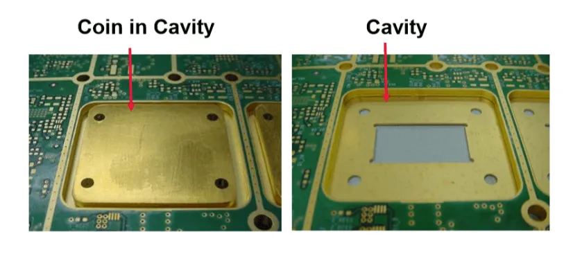
Cavity PCB refers to a printed circuit board with recessed areas that accommodate components, improve electrical performance, or enhance thermal dissipation. These cavities are intentionally designed within the PCB structure, allowing components to be placed deeper into the board for a lower overall profile.
There are three main types of cavities in Cavity PCB design:
-
Shallow Cavities: Minor recesses for reducing component height.
-
Deep Cavities: Larger cutouts for housing thick components or improving thermal management.
-
Embedded Cavities: Fully enclosed spaces for integrating chips or passive components within the PCB layers.
Unlike standard PCB designs, Cavity PCB provides enhanced mechanical stability, better heat dissipation, and improved RF performance, making it ideal for high-frequency and power applications.

Why Use Cavity PCBs?
Cavity PCB offers significant advantages in modern electronics by optimizing electrical, thermal, and mechanical performance.
-
RF and Microwave Applications: Cavity PCB helps reduce signal interference by controlling parasitic effects and minimizing unwanted resonances. This makes it ideal for high-frequency communication, radar systems, and RF modules.
-
Thermal Management: By incorporating cavities, heat-generating components can be placed closer to heat sinks or metal cores, improving thermal dissipation and ensuring stable performance in power electronics.
-
Component Integration: Cavity PCB allows embedding of chips, sensors, or passive components within the board structure, reducing assembly complexity and enabling compact, high-density designs.
-
Mechanical Benefits: The recessed design improves structural integrity while lowering the overall PCB thickness, making it suitable for space-constrained applications like mobile devices and aerospace electronics.

PCB Cavity Design Considerations
Effective Cavity PCB design requires careful planning to optimize performance and reliability.
-
Cavity Depth and Placement: The depth and position of the cavity must be precisely controlled to maintain material integrity and ensure proper alignment with components, preventing mechanical stress or warping.
-
Trace-to-Cavity Distance: Maintaining adequate spacing between traces and the cavity edge is crucial to avoid signal interference and degradation, especially in high-frequency circuits.
-
Resonant Cavity Effects: Unwanted electromagnetic resonance can occur in RF applications. Proper design adjustments, such as cavity shaping and shielding, help mitigate these effects for stable signal transmission.
-
Material Selection: Choosing suitable dielectric and core materials is essential to ensure durability, thermal stability, and optimal electrical performance, particularly in high-power or RF-sensitive Cavity PCB designs.
Manufacturing Methods for Cavity PCBs
Producing a high-quality Cavity PCB requires specialized manufacturing techniques to achieve precision and reliability.
-
Milling and Routing: CNC machining is commonly used to create cavities with high precision, ensuring accurate depth and smooth edges without damaging the PCB structure.
-
Sequential Lamination: This technique involves stacking and laminating multiple PCB layers to embed cavities within the board, allowing for complex multilayer designs with integrated components.
-
Laser Drilling: Advanced laser technology enables the formation of fine-pitched cavities, especially for high-density applications requiring micro-level precision.
-
Metal Core and Copper-Filled Cavities: For applications requiring superior thermal management and RF performance, metal core PCBs or copper-filled cavities are used to enhance heat dissipation and minimize signal loss.
Application of Solder Paste in PCB Cavities
Proper solder paste application is critical in Cavity PCB assembly to ensure reliable electrical connections and mechanical stability.
-
Importance of Proper Solder Paste Application: Precise solder paste deposition ensures strong bonding between components and pads, preventing connectivity issues in recessed areas.
-
Techniques for Reliable Soldering: Stencil printing with controlled paste volume, jet dispensing for precise placement, and reflow soldering with optimized temperature profiles help achieve consistent results in cavity regions.
-
Avoiding Defects: To prevent voids, insufficient solder, or uneven distribution, techniques like vacuum-assisted reflow, controlled stencil thickness, and optimized solder paste formulations are used to enhance reliability and performance.

Special Cavity PCB Types
There are several specialized types of Cavity PCBs designed to meet specific performance and application needs.
-
Die Cavity Copper Metal Core PCBs: These PCBs integrate a metal core within the cavity to improve thermal conductivity, making them ideal for applications with high power dissipation, such as power electronics and LEDs.
-
Embedded Cavity PCBs: These designs embed components such as chips or passives within the PCB layers, providing compact packaging solutions for high-density applications like mobile devices or automotive electronics.
-
RF Cavity PCBs and Resonator Cavity Designs: Used in RF applications, these PCBs are engineered to optimize signal integrity and minimize interference by controlling resonance effects and ensuring stable performance in high-frequency circuits.
-
Cavity Filter PCBs: These specialized designs are used to filter unwanted frequencies, enhancing the performance of high-frequency signal processing systems, such as communication devices and radar systems.
Get a Quotation For Cavity PCB Now
Challenges and Solutions in Cavity PCB Manufacturing
Cavity PCB manufacturing presents unique challenges that require precise techniques and careful consideration of material properties and design features.
-
Material Handling: During manufacturing, materials can be prone to deformation or delamination, especially when cavities are deep or components are embedded. Using high-quality, stable materials and controlled lamination processes helps prevent such issues.
-
Alignment Issues: Achieving accurate cavity depth and proper positioning is crucial to prevent functional or structural defects. Advanced CNC machines, laser drilling, and precise measurement tools ensure that cavities are correctly aligned and meet design specifications.
-
Cavity Resonance Control: Cavity resonance can cause unwanted electromagnetic effects, especially in RF and high-frequency applications. This can be mitigated through careful cavity shape optimization, shielding, and proper placement of components to avoid interference and maintain signal integrity.
Get a Quotation For Cavity PCB Now
Cavity PCB Technology: A Key Breakthrough for Enhanced Performance and Integration
Cavity PCB technology is increasingly being used in high-performance applications such as 5G, automotive radar, and high-frequency communication systems. Its ability to reduce interference, control impedance, and enhance signal integrity makes it essential for these demanding environments.
Advancements in embedded component integration are enabling more compact and efficient designs. By embedding chips, sensors, or passive components within the PCB layers, space is saved, and component interconnections are simplified, leading to more reliable and high-density designs.
In parallel, improved manufacturing techniques are allowing for finer cavity control. Methods like precision milling, laser drilling, and advanced lamination techniques are being refined, ensuring more accurate cavity formation. This not only improves the electrical and mechanical properties of the PCB but also supports the development of more complex, high-performance applications.
Contact Us NOW

