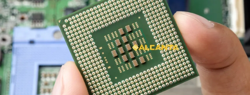
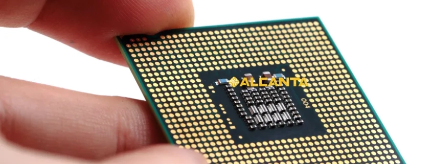
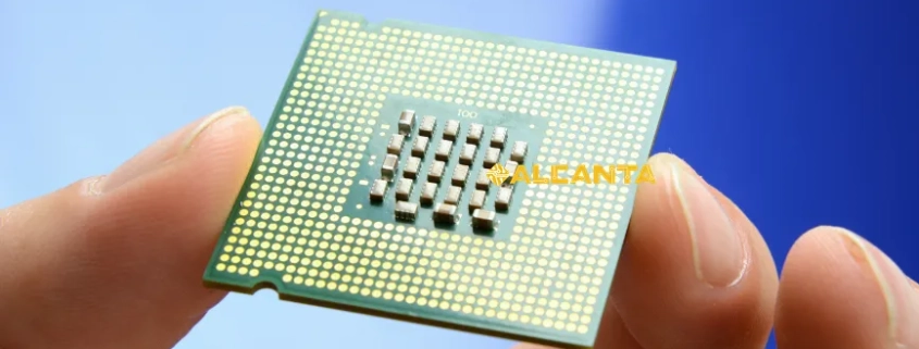
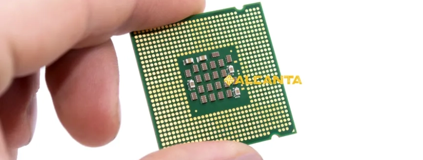
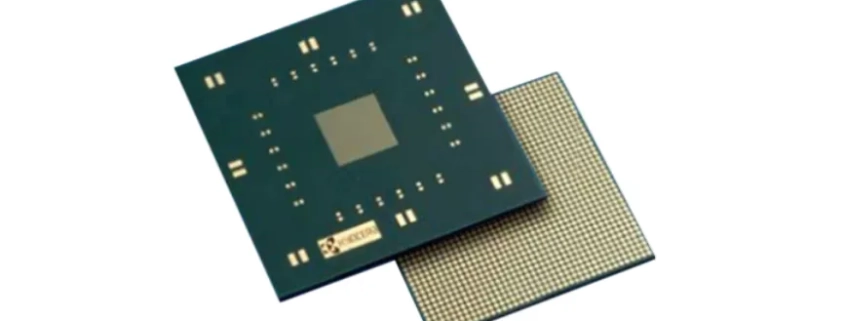
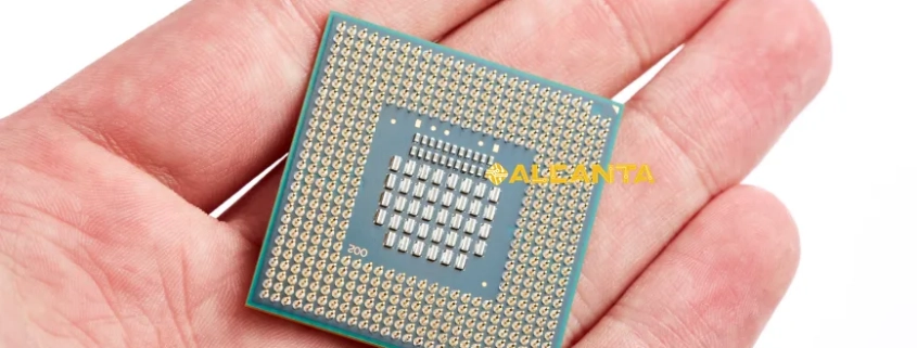
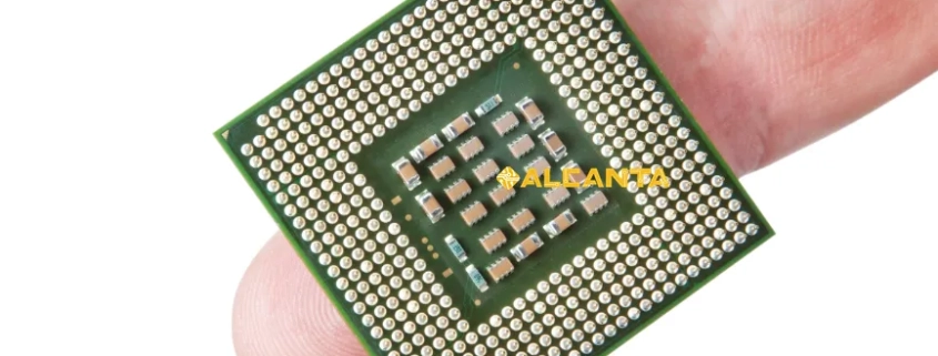
COB LED, or Chip on Board LED, represents a revolutionary advancement in lighting technology, consolidating multiple LED chips onto a single substrate. Its significance in the lighting industry lies in its ability to offer unparalleled energy efficiency, exceptional brightness, and unmatched reliability. Unlike traditional LEDs, COB LEDs produce more lumens per watt, making them highly energy-efficient and cost-effective. Moreover, their compact design enables higher brightness levels, ensuring superior illumination in various applications. Additionally, COB LEDs boast enhanced reliability due to their simplified construction, minimizing potential failure points. Overall, COB LED stands as a beacon of innovation, driving efficiency and performance to new heights in the lighting sector.
阅读更多Printed Circuit Boards (PCBs) are the backbone of modern electronics, providing a platform for interconnecting electronic components to form functional devices. Their importance in electronic devices cannot be overstated, as they enable the efficient flow of electricity and data within intricate electronic systems. Within the PCB fabrication process, UV exposure plays a pivotal role. It serves as a critical step in defining the circuit patterns on the PCB substrate. Understanding what is the UV exposure effect on the PCB substrate is paramount for ensuring the accuracy and reliability of the final product. In this article, we delve into the intricate relationship between UV exposure and PCB substrates, exploring its implications and significance in electronic manufacturing.
阅读更多In today’s era of rapid technological advancement, integrated circuits (ICs) serve as the backbone of modern electronics. These miniature electronic components, also known as microchips, play a pivotal role in powering various devices, from smartphones and computers to medical equipment and automotive systems. Integrated circuits integrate multiple electronic components onto a single semiconductor chip, enabling compact designs, enhanced performance, and reduced power consumption.
Within the realm of integrated circuits, the choice of chip carrier package significantly influences the functionality and reliability of the IC. Plastic Leaded Chip Carrier (PLCC) emerges as a prominent solution, offering robust protection and efficient mounting for ICs. As we delve deeper into understanding PLCC, we uncover its crucial role in safeguarding and facilitating the operation of integrated circuits across diverse applications.
阅读更多
In the realm of modern electronics, transparent PCB substrates hold a pivotal role, offering not just functionality but also aesthetic appeal. As technology advances, there’s a growing demand for sleek, transparent designs in various electronic devices, from smartphones to automotive displays. The substrate material, often overlooked, plays a critical role in ensuring the performance and reliability of PCBs. It serves as the foundation upon which components are mounted and interconnected, influencing electrical properties, thermal management, and overall durability. Understanding the significance of transparent PCB substrates and selecting the appropriate material is paramount in achieving desired transparency while maintaining functionality and reliability in electronic designs.
ABF substrate, short for Ajinomoto Build-up Film substrate, is a critical component in semiconductor packaging. It serves as a foundation for mounting and connecting semiconductor chips within electronic devices. ABF substrates consist of multiple layers of insulating material with embedded conductive traces, providing pathways for electrical signals to travel between components.
The significance of ABF substrate lies in its ability to support miniaturization and enhance the performance of electronic devices. Its high-density interconnection capability enables efficient signal transmission, contributing to faster processing speeds and improved overall functionality. As semiconductor technology continues to advance, the demand for ABF substrates grows, making them indispensable in the development of cutting-edge electronic products.
阅读更多PCB substrates, fundamental to modern electronics, serve as the backbone of electronic devices, providing structural support and electrical insulation. Understanding what PCB substrate entails is crucial for comprehending the intricacies of electronic design and manufacturing processes. These substrates play a pivotal role in ensuring the functionality, reliability, and performance of electronic circuits. Selecting the appropriate substrate material is paramount in PCB fabrication, as it directly impacts the circuit’s thermal management, signal integrity, and mechanical stability. In this guide, we delve into what PCB substrates are, their diverse types, composition, fabrication process, and the critical factors to consider when choosing the right substrate material for specific applications.
阅读更多ABF substrate, short for Anisotropic Conductive Film, stands as a cornerstone in modern electronics manufacturing. As an essential element in the production of electronic devices, it facilitates the interconnection of various components with precision and reliability. In this article, we delve into the intricate world of ABF substrate manufacturers, unraveling their pivotal role in sustaining the electronics industry’s momentum. From their technological advancements to their contributions towards meeting the escalating demand for electronic products, understanding the landscape of ABF substrate manufacturers is crucial for comprehending the dynamics driving innovation and progress in electronics manufacturing.
Ajinomoto ABF substrates represent a cutting-edge advancement in semiconductor manufacturing. These substrates, developed by Ajinomoto Fine-Techno, offer unparalleled performance and reliability, revolutionizing the way electronic devices are produced. ABF substrates play a crucial role in semiconductor manufacturing processes, serving as the foundation for integrated circuits and electronic components. Their significance lies in their ability to provide high-density interconnections, superior thermal management, and enhanced electrical properties, ultimately enabling the creation of smaller, faster, and more energy-efficient devices. As the demand for advanced electronics continues to rise, the importance of ABF substrates in driving innovation and meeting industry requirements cannot be overstated.
阅读更多ABF (Ajinomoto Build-up Film) substrates serve as crucial components in the semiconductor industry, facilitating the interconnection of integrated circuits within electronic devices. These substrates consist of thin layers of insulating material, typically made of polyimide, with embedded copper traces for electrical connections. ABF substrates play a vital role in enhancing the performance, reliability, and miniaturization of semiconductor devices. They offer superior thermal and mechanical properties, enabling high-speed data transmission and efficient heat dissipation. As semiconductor technology advances, the demand for ABF substrates continues to rise, driven by the need for more compact and powerful electronic devices. Consequently, understanding the significance and evolution of ABF substrates is paramount in comprehending the trajectory of the semiconductor industry.
阅读更多The ABF (Ajinomoto Build-Up Film) substrate market plays a pivotal role in the electronics industry, serving as a crucial component in electronic packaging and interconnection technologies. ABF substrates offer numerous advantages over traditional materials, including enhanced electrical performance, thermal conductivity, and reliability. As the demand for smaller, faster, and more reliable electronic devices continues to rise, the importance of ABF substrates becomes increasingly evident. This blog aims to delve into the ABF substrate market share, offering comprehensive insights into its size, competitive landscape, product features, and future prospects, thereby facilitating a deeper understanding of this vital segment within the electronics industry.
CONTACT US
4th Floor, A3 Building, HuaFeng Industrial Park, GuanTian Village, BeiHuan Road, ShiYan Street, Bao An District, Shenzhen City, Guangdong Province, China
Tel:086 (0)755-8524-1496
WhatsApp: 8615014077679
Skype: Henrychinasz
📧 pcb@alcantapcb.com
CONTACT US
SHIPPING
CERTIFCATION
recent articles
- Small Outline Integrated Circuit(SOIC) in PCB Design2025-03-12 - 2:43 上午
- TSOP/LOC Lead Frame and Its Role in Semiconductor Packaging2025-03-11 - 2:38 上午
- Key Benefits of Plastic Leaded Chip Carrier (PLCC) Lead Frame2025-03-10 - 2:47 上午
- Advantages of Plastic Dual In-line Package(PDIP) Lead Frame2025-03-07 - 3:03 上午