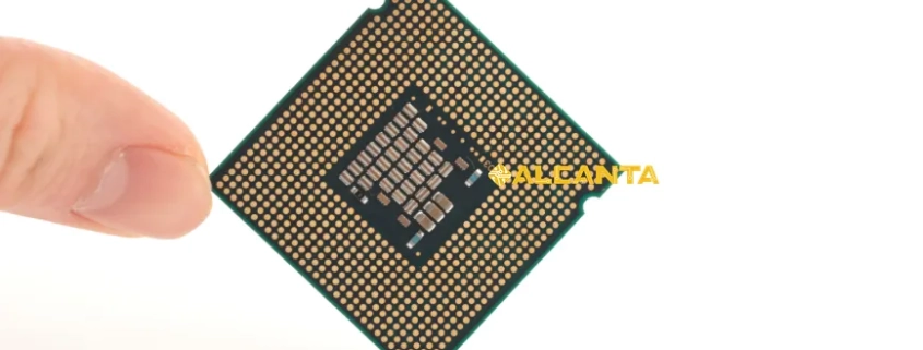
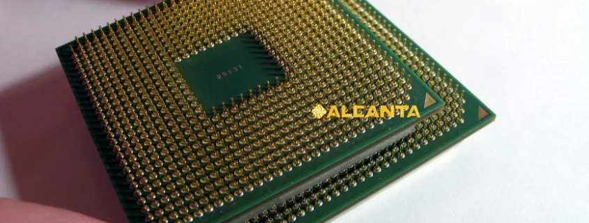
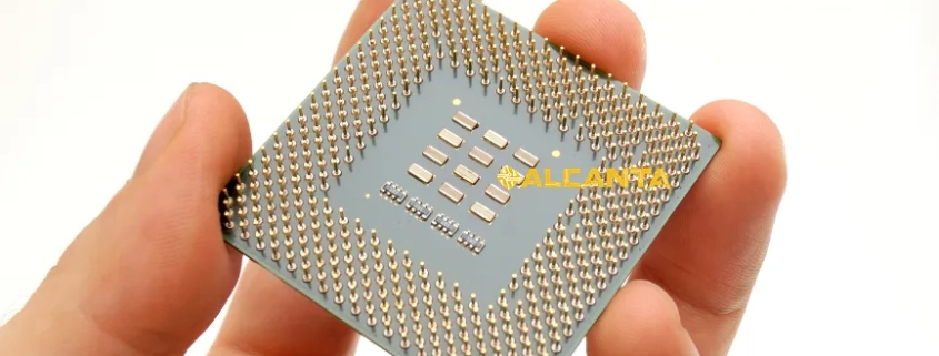
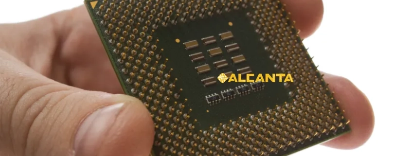
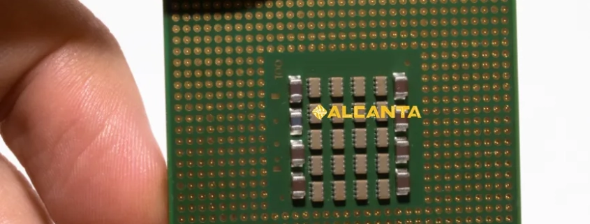
Chip Scale Package (CSP) technology plays a pivotal role in the miniaturization and enhancement of electronic devices across various industries. Its significance lies in its ability to offer compact packaging solutions without compromising performance, making it ideal for applications where space constraints are critical. In this article, we will delve into the fundamentals of CSP, exploring its evolution, manufacturing processes, and comparison with other packaging technologies. Additionally, we will examine the diverse application domains of CSP, ranging from mobile devices to automotive electronics, highlighting its versatility and impact. Through this exploration, readers will gain insights into the pivotal role of CSP in shaping the future of integrated circuit packaging.
阅读更多Semiconductor packaging stands as a critical aspect of the integrated circuit (IC) industry, facilitating the protection, interconnection, and heat dissipation of semiconductor chips. Within this landscape, the Dual In-Line Package (DIP) emerges as a foundational pillar. Its historical importance traces back to the infancy of electronic devices, marking a pivotal advancement in miniaturization and connectivity. As the precursor to modern packaging technologies, DIP revolutionized electronic manufacturing, enabling the mass production of ICs. Its enduring legacy underscores its significance in shaping the evolution of electronic devices, laying the groundwork for the intricate and compact designs prevalent in today’s tech-driven world.
阅读更多Transistors serve as fundamental building blocks in electronic devices, facilitating the amplification and switching of electrical signals. Their miniature size and efficiency make them indispensable in modern technology, powering everything from smartphones to spacecraft. However, the effectiveness of transistors relies not only on their internal structure but also on how they are packaged. Transistor packaging plays a pivotal role in safeguarding these delicate components from environmental hazards, dissipating heat effectively, and enabling easy integration into circuitry. Understanding the significance of transistor packaging is crucial for engineers and designers, as it directly impacts the performance, reliability, and longevity of electronic systems. In this blog, we delve into the diverse world of transistor package types, unraveling their characteristics and applications to empower readers in making informed decisions in electronic design.
阅读更多SMD LED chips stand at the forefront of modern lighting technology, serving as pivotal components in an array of applications. As we delve into this topic, we’ll uncover the intricate features, versatile applications, and precise technical specifications of SMD LED chips. These tiny yet powerful devices have revolutionized illumination, offering unparalleled efficiency, durability, and flexibility. Join us on a journey to explore the remarkable characteristics and myriad uses of SMD LED chips, shedding light on their indispensable role in shaping the future of lighting solutions.
阅读更多The Dual Inline Package (DIP) stands as a hallmark in the realm of integrated circuit (IC) packaging, symbolizing a pivotal era in electronics. Its inception marked a transformative shift, revolutionizing the way ICs were housed and utilized. This blog embarks on a journey to unravel the historical significance and enduring relevance of the DIP in the landscape of IC products. We will delve into the structural intricacies of the DIP, uncover its inherent advantages, and explore its versatile applications across various industries. Additionally, we will compare it with contemporary packaging solutions like the Small Outline Integrated Circuit (SOIC), shedding light on the timeless appeal of the DIP. Join us as we navigate through the corridors of technology, tracing the evolution and impact of this iconic packaging format.
阅读更多In today’s electronics manufacturing, Surface Mount Device (SMD) components play a pivotal role due to their compact size, reliability, and ease of assembly. These components, including resistors and capacitors, are directly mounted onto the surface of printed circuit boards (PCBs), eliminating the need for traditional through-hole soldering. Among the various SMD sizes, the 0805 package stands out for its versatility and widespread usage. Its importance lies in its balance between size and handling, making it suitable for a wide range of applications in consumer electronics, industrial equipment, automotive systems, and more. Understanding the significance of the 0805 package is crucial for engineers and hobbyists alike in designing efficient and compact electronic devices.
阅读更多Semiconductor packaging plays a pivotal role in safeguarding integrated circuits (ICs) while facilitating their integration into electronic systems. Among the myriad packaging styles, Quad Flat Package (QFP) stands out as a prominent choice within the electronics industry. Characterized by its flat and square shape with leads extending from all four sides, QFP offers a balance of performance, reliability, and space efficiency. As an enduring solution, QFP has found widespread adoption across various applications, owing to its versatility and adaptability to diverse electronic designs.
阅读更多In the realm of modern electronics, On Board Chip (OBC) technology stands as a cornerstone, revolutionizing the way electronic devices are designed and manufactured. At its essence, OBC refers to the integration of semiconductor chips directly onto a circuit board, eliminating the need for traditional packaging methods. This approach offers numerous advantages, including compactness, improved thermal management, and heightened reliability. Key terms such as Chip on Board (COB), Flip Chip, and Multi Chip Module (MCM) are integral to understanding the intricacies of OBC technology. As electronic devices continue to evolve and demand compactness without compromising performance, the significance of OBC technology becomes increasingly pronounced, shaping the landscape of modern electronics.
阅读更多LED lighting technology has witnessed remarkable advancements since its inception. Initially discovered in the early 20th century, LEDs were primarily used as indicator lights. However, with ongoing research and development, LED technology has evolved into a leading lighting solution renowned for its energy efficiency, longevity, and versatility.
Over the years, the LED industry has seen significant breakthroughs in efficiency, brightness, and color rendering, making it a preferred choice for various lighting applications. From residential and commercial spaces to automotive and entertainment industries, LEDs have revolutionized the way we illuminate our surroundings.
In this blog, we delve into one of the innovative developments in LED technology – Chip on Board (COB) LED lights. We will explore the structure, working principle, advantages, applications, and lifecycle of COB LED lights, providing readers with valuable insights into this cutting-edge lighting solution.
阅读更多With the increasing popularity of LED technology and its expanding applications across various sectors, the demand for efficient and reliable lighting solutions has surged. In response to this demand, LED chip boards have emerged as crucial components in the realm of LED lighting. These boards play a pivotal role in providing illumination with enhanced brightness, energy efficiency, and longevity. As the lighting industry continues to evolve, LED chip boards stand out as innovative solutions that offer versatility and superior performance. In this blog, we will delve deeper into the concept of LED chip boards, exploring their functionalities, advantages, and diverse applications in today’s lighting landscape.
阅读更多CONTACT US
4th Floor, A3 Building, HuaFeng Industrial Park, GuanTian Village, BeiHuan Road, ShiYan Street, Bao An District, Shenzhen City, Guangdong Province, China
Tel:086 (0)755-8524-1496
WhatsApp: 8615014077679
Skype: Henrychinasz
📧 pcb@alcantapcb.com
CONTACT US
SHIPPING
![]()
CERTIFCATION
![]()
recent articles
 Copper Core PCB vs Aluminium Core PCB Explained2025-09-18 - 7:13 上午
 Microwave PCB Manufacturers | RF Design and Fabrication2025-09-16 - 7:58 上午
 Flex PCB Manufacturing Process: Step-by-Step Guide2025-09-10 - 6:59 上午
 PCB Lamination Process & Sequential Lamination2025-09-04 - 8:10 上午

