
Elevating BGA Reliability: Substrate Plating Insights
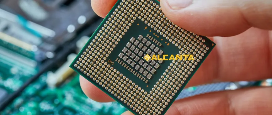
In today’s advanced electronic landscape, Ball Grid Array (BGA) technology stands as a cornerstone for compact and high-performance electronic devices. BGA facilitates the dense packaging of integrated circuits (ICs) onto a single substrate, enhancing functionality while minimizing space requirements. However, amidst the intricate network of connections and components, the substrate plays a pivotal role. Serving as the foundation that hosts and interconnects various components, the substrate ensures structural integrity, electrical connectivity, and thermal management within BGA packages. Understanding the significance of the substrate is crucial for grasping the reliability and performance of BGA technology, making it a vital aspect of modern electronic manufacturing and design processes.
Understanding BGA Substrate
In the realm of Ball Grid Array (BGA) technology, the substrate stands as a fundamental component, serving multiple critical functions. Essentially, the substrate is a supportive platform that not only physically houses the integrated circuit (IC) but also provides electrical connectivity and thermal dissipation.
The substrate in BGA technology acts as a conduit for electrical signals, facilitating communication between the IC and other components within the package. Moreover, it offers structural support to the IC and helps dissipate heat generated during operation, thus ensuring optimal performance and reliability.
When comparing package substrate and IC substrate, it’s important to note their distinct roles. The package substrate primarily serves as the interface between the IC and the rest of the electronic system, providing the necessary electrical connections and mechanical support. On the other hand, the IC substrate, also known as the chip carrier or interposer, directly supports the IC, providing a platform for mounting and interconnecting the silicon die.
While both substrates play vital roles in BGA technology, they differ in design and functionality, with the package substrate focusing more on external connectivity and the IC substrate being integral to the IC itself. Understanding these differences is crucial for designing robust and efficient BGA packages.
Exploring BGA vs. FBGA
BGA (Ball Grid Array) Technology:
BGA technology revolutionized electronic packaging by introducing a compact and efficient method for mounting integrated circuits (ICs) onto substrates. In BGA packages, solder balls are arranged in a grid pattern on the underside of the IC, providing a robust electrical connection to the substrate. This design offers several advantages, including improved electrical performance, reduced signal distortion, and enhanced thermal dissipation.
Differentiating Features between BGA and FBGA (Fine Ball Grid Array):
While both BGA and FBGA (Fine Ball Grid Array) share similarities in their underlying principles, they exhibit distinct features:
1. Ball Pitch: One of the primary differences lies in the ball pitch—the distance between adjacent solder balls. FBGA typically features a smaller pitch compared to traditional BGAs, allowing for higher-density packaging and finer-pitched interconnections.
2. Miniaturization: FBGA packages are designed for miniaturization and high-density applications, with smaller dimensions and finer ball pitches than standard BGAs. This enables the integration of more components into a smaller footprint, making FBGA ideal for space-constrained designs.
3. Performance: While both BGA and FBGA offer reliable electrical connections, FBGA’s finer pitch enables superior electrical performance, including reduced signal crosstalk and improved high-speed signal integrity. This makes FBGA well-suited for high-performance applications such as high-speed computing and telecommunications.
4. Manufacturing Complexity: Due to their finer pitch and tighter tolerances, FBGA packages require more advanced manufacturing processes and equipment compared to traditional BGAs. This can result in higher manufacturing costs but offers superior performance and miniaturization benefits.
Understanding the differences between BGA and FBGA is crucial for selecting the most suitable packaging solution based on specific application requirements, balancing factors such as cost, performance, and form factor.
BGA Soldering Process
The soldering process of Ball Grid Array (BGA) packages is a critical step in the assembly of modern electronic devices. It involves the attachment of the BGA chips onto a printed circuit board (PCB) using tiny solder balls that are pre-attached to the underside of the package. This process is delicate and requires precision to ensure both functionality and reliability.
Overview of BGA Soldering Techniques:
1. Reflow Soldering: The most common technique used for BGA soldering is reflow soldering. This method involves placing the BGA with its solder balls aligned on the corresponding pads of the PCB. The entire assembly is then heated in a reflow oven where the temperature is carefully controlled to melt the solder without damaging the components. The melting solder creates permanent joints between the BGA and the PCB pads as it cools and solidifies.
2. X-Ray Inspection: Post-soldering, X-ray inspection is often used to examine the solder joints beneath the BGA packages since they are not visible from the outside. This inspection ensures that all connections are correctly formed and there are no defects such as bridges or cold joints, which could compromise the device’s performance.
3. Rework Stations: For any repairs or adjustments after initial soldering, specialized BGA rework stations are used. These stations allow for precise de-soldering and re-soldering of BGAs, which is essential for maintaining the integrity of the PCB and the chip itself during rework processes.
Importance of Proper Soldering for BGA Reliability:
Proper soldering in BGA assembly is crucial for several reasons:
1. Electrical Connectivity: Adequate soldering ensures that all electrical connections between the BGA and the PCB are robust and consistent. This is vital for the stable operation of the ICs and the overall device functionality.
2. Thermal Management: Effective solder joints help in dissipating heat generated by the IC during operation. Good thermal connectivity helps in maintaining optimal temperatures and prevents overheating, thereby extending the lifespan of the device.
3. Mechanical Stability: Strong solder joints provide mechanical stability to the BGA against physical stresses such as vibrations and drops, which are common in mobile devices and handheld electronics.
4. Long-Term Reliability: Properly executed soldering reduces the likelihood of joint failures over time due to thermal cycling and other environmental factors. This reliability is critical for devices expected to have long service lives or operate under harsh conditions.
In conclusion, mastering BGA soldering techniques is essential for ensuring the high performance and reliability of electronic assemblies. Manufacturers must continuously refine their soldering processes to keep pace with the increasing complexity of electronic devices and their requirements for durability and performance.
The BGA Attach Process
The BGA attach process is a meticulous procedure crucial for the reliable assembly of electronic devices. Here’s a detailed step-by-step explanation:
1. Preparation: Before attaching the BGA, the substrate and the BGA itself must be thoroughly inspected for any defects or contaminants. Proper cleaning and surface preparation ensure optimal solderability.
2. Alignment: The BGA is precisely aligned on the substrate, ensuring that the solder balls align with the corresponding pads on the substrate. This alignment is critical for establishing proper electrical connections.
3. Solder Paste Application: Solder paste, a mixture of flux and solder particles, is applied to the pads on the substrate. The solder paste serves as the medium through which the solder balls on the BGA will attach to the substrate during the reflow process.
4. Placement: The BGA is carefully placed onto the substrate, aligning it with the solder paste-covered pads. Precision equipment such as pick-and-place machines or automated assembly systems may be used to ensure accurate placement.
5. Reflow Soldering: The assembled substrate and BGA undergo reflow soldering, typically in a controlled atmosphere oven. During reflow, the solder paste melts, forming solder joints between the BGA solder balls and the substrate pads. Proper temperature profiles are crucial to ensure complete solder reflow and avoid defects like solder bridges or cold joints.
6. Cooling and Inspection: After reflow, the assembly is allowed to cool to solidify the solder joints. Visual inspection and, in some cases, X-ray inspection are performed to ensure the integrity of the solder joints and detect any defects.
7. Cleaning: If necessary, the assembly may undergo cleaning to remove any flux residues or contaminants left from the soldering process. Proper cleaning helps prevent corrosion and ensures long-term reliability.
Key Factors Influencing Successful BGA Attachment:
1. Solder Paste Quality: The quality and consistency of the solder paste directly impact the integrity of the solder joints. High-quality solder paste with appropriate particle size distribution and flux activity is essential for reliable attachment.
2. Alignment Accuracy: Precise alignment between the BGA and the substrate is critical to ensure proper electrical connections and avoid misalignment-related defects.
3. Reflow Profile: The reflow temperature profile must be carefully controlled to ensure complete solder reflow without overheating or thermal damage to the components. Proper temperature ramp-up, soaking, and cooling rates are essential for achieving reliable solder joints.
4. Surface Finish: The surface finish of both the substrate pads and the BGA solder balls affects solder wetting and joint formation. Common surface finishes include electroless nickel immersion gold (ENIG), solder immersion, and organic solderability preservatives (OSP).
5. Component Handling: Proper handling and storage of BGAs and substrates are crucial to prevent damage or contamination that could affect solderability and attachment reliability.
By meticulously following these steps and considering key factors, manufacturers can ensure the successful attachment of BGAs, resulting in reliable electronic assemblies with optimal performance and longevity.
Introducing BGA Substrate Plating
BGA Substrate Plating:
BGA substrate plating refers to the process of applying thin layers of metal onto the substrate surface to enhance its electrical conductivity, solderability, and durability. This plating is typically applied to the copper traces and pads on the substrate, which serve as the electrical interconnects between the BGA package and the rest of the electronic system.
Significance of BGA Substrate Plating:
BGA substrate plating plays a crucial role in ensuring the reliability and performance of BGA packages:
1. Enhanced Electrical Conductivity: The plated layers improve the conductivity of the substrate, reducing electrical resistance and signal losses. This is vital for maintaining signal integrity and minimizing transmission errors in high-speed electronic devices.
2. Improved Solderability: Proper plating promotes the formation of robust solder joints during the attachment of the BGA to the substrate. The plated surfaces provide better wetting characteristics, ensuring uniform solder spread and strong adhesion between the solder balls and the substrate pads.
3. Corrosion Resistance: Plating serves as a protective barrier against corrosion, preventing oxidation of the substrate and solder joints over time. This helps maintain the integrity of the electrical connections and prolongs the lifespan of the electronic assembly, especially in harsh operating environments.
4. Thermal Management: Some plating materials, such as thermal conductive metals like copper or silver, can aid in heat dissipation from the BGA package. This is particularly beneficial for devices with high power dissipation requirements, as it helps prevent thermal buildup and potential performance degradation.
Importance of Proper Plating for BGA Reliability and Performance:
Proper plating is essential for ensuring the reliability and performance of BGA packages:
1. Reliability: Adequate plating prevents common failure modes such as solder joint fatigue, open circuits, and electrical shorts, which can compromise the functionality and lifespan of the electronic device.
2. Signal Integrity: Well-plated substrates minimize signal degradation and electromagnetic interference, preserving the integrity of high-speed data and communication signals.
3. Manufacturability: Properly plated substrates facilitate the assembly process by promoting consistent soldering and reducing the likelihood of defects, leading to higher manufacturing yields and lower production costs.
4. Customer Satisfaction: Reliable BGA packages with robust substrate plating contribute to overall customer satisfaction by delivering electronic products with superior performance, durability, and longevity.
In summary, BGA substrate plating is a critical aspect of electronic packaging, ensuring the integrity, reliability, and performance of BGA assemblies. Manufacturers must carefully select and apply plating materials and processes to meet the demanding requirements of modern electronic devices.
FAQs about bga substrate plating
The substrate in BGA (Ball Grid Array) is a supportive platform that hosts and interconnects various components of the integrated circuit (IC) package. It provides structural integrity, electrical connectivity, and thermal management within BGA packages.
The difference between BGA and FBGA (Fine Ball Grid Array) lies primarily in the ball pitch, with FBGA typically featuring a smaller pitch. FBGA is designed for higher-density packaging and finer-pitched interconnections compared to traditional BGAs.
BGA is soldered using a technique called reflow soldering. This process involves placing the BGA with its solder balls aligned on corresponding pads of the printed circuit board (PCB). The assembly is then heated in a controlled atmosphere oven, causing the solder to melt and form permanent joints between the BGA and the PCB pads.
The BGA attach process involves several steps:
Preparation: Inspecting and cleaning the substrate and BGA.
Alignment: Precisely aligning the BGA on the substrate, ensuring proper electrical connections.
Solder Paste Application: Applying solder paste to the substrate pads.
Placement: Placing the BGA onto the substrate, aligning it with the solder paste-covered pads.
Reflow Soldering: Heating the assembly to melt the solder and form solder joints between the BGA and the substrate.
Cooling and Inspection: Allowing the assembly to cool and inspecting for defects or irregularities in the solder joints.

