
Deciphering the Core: BGA Substrate Layers Explored
In today’s rapidly evolving electronics landscape, Ball Grid Array (BGA) packaging stands as a cornerstone of innovation. With its compact design and efficient heat dissipation, BGA has become ubiquitous in various electronic devices, from smartphones to high-performance computing systems. However, the true essence of BGA lies within its substrate layers, which serve as the foundation for this advanced packaging technology. These substrate layers play a pivotal role in providing structural integrity, electrical connectivity, and thermal management within the BGA package, ultimately ensuring the reliability and performance of modern electronic devices. Understanding the intricacies of BGA substrate layers is essential for comprehending the inner workings and potential applications of this groundbreaking packaging technology.
Understanding BGA Substrate
In the realm of Ball Grid Array (BGA) packaging, the substrate serves as the fundamental platform upon which the entire assembly is built. Essentially, the substrate acts as a bridge, connecting the silicon die to the external world through its intricate network of traces and vias. Its primary role encompasses electrical interconnection, mechanical support, and thermal dissipation.
1. Definition and Role: The substrate in a BGA package is a thin, rigid board typically made of materials like fiberglass-reinforced epoxy resin (FR-4) or more advanced materials like organic substrates or coreless substrates. It provides a stable foundation for mounting the silicon die and facilitates the transfer of signals and power between the die and the package’s external pins or balls. Additionally, it helps manage the heat generated by the integrated circuits during operation, enhancing the overall reliability of the package.
2. Types of Substrates: BGA packages utilize various types of substrates tailored to meet specific performance and cost requirements. Organic substrates, consisting of epoxy resin and woven glass fabric, are widely used due to their excellent electrical properties and cost-effectiveness. Coreless substrates, on the other hand, eliminate the traditional fiberglass core, resulting in thinner and lighter packages with enhanced electrical performance and thermal dissipation capabilities. Other specialized substrates, such as ceramic or silicon-based substrates, are utilized in high-end applications demanding superior electrical performance and reliability.
3. Comparison of Substrate Materials: Each substrate material offers distinct advantages and trade-offs. Organic substrates strike a balance between cost-effectiveness and performance, making them suitable for a wide range of consumer electronics applications. Coreless substrates offer improved electrical performance and thermal management, albeit at a higher cost. Ceramic substrates excel in high-frequency applications due to their superior electrical properties, while silicon-based substrates offer exceptional thermal conductivity for demanding thermal management requirements.
Understanding the characteristics and properties of different substrate materials is crucial in selecting the most appropriate solution for a particular BGA application, ensuring optimal performance and reliability.
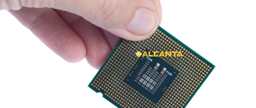
Components of BGA Package
Within a Ball Grid Array (BGA) package, several components work in harmony to facilitate the reliable operation of integrated circuits. Understanding each element’s role is essential for appreciating the complexity and functionality of BGA packaging.
1. Silicon Die: At the heart of the BGA package lies the silicon die, which houses the integrated circuits responsible for processing data and executing instructions. The die is typically mounted onto the substrate using wire bonding or flip-chip technology, forming electrical connections to the substrate’s traces.
2. Substrate Layers: The substrate serves as the foundation for the BGA package, providing mechanical support and electrical connectivity between the silicon die and the package’s external pins or balls. It consists of multiple layers, including signal and power planes, routing traces, vias, and solder mask, meticulously designed to ensure optimal signal integrity and thermal performance.
3. Solder Balls: Solder balls are strategically positioned on the underside of the BGA package, forming a grid-like array that interfaces with the printed circuit board (PCB) or other mounting surfaces. These solder balls facilitate electrical connections between the BGA package and the external circuitry while also providing mechanical support and thermal conductivity.
4. Underfill Material: In many BGA packages, a layer of underfill material is applied between the silicon die and the substrate to enhance mechanical strength, prevent solder joint cracking, and improve thermal cycling reliability. This epoxy-based material fills the gap between the die and the substrate, ensuring uniform stress distribution and minimizing the risk of delamination or package warpage.
5. Encapsulant: Some BGA packages incorporate an encapsulant material to protect the silicon die and wire bonds from external environmental factors such as moisture, dust, and mechanical shocks. This encapsulant, typically a thermosetting polymer, encapsulates the entire assembly, providing additional mechanical stability and safeguarding the sensitive electronic components from damage.
Each component within the BGA package plays a crucial role in ensuring the reliability and performance of the integrated circuits. The silicon die forms the core processing unit, while the substrate layers facilitate electrical connectivity and thermal management. Solder balls enable seamless integration with external circuitry, while underfill and encapsulant materials enhance mechanical robustness and environmental resilience. By harmonizing these components, BGA packages deliver high-performance solutions for a diverse range of electronic applications, from consumer electronics to aerospace systems.
Exploring Inside a BGA
Delving into the inner workings of a Ball Grid Array (BGA) package unveils a meticulously engineered structure designed to optimize performance and reliability. Let’s take a step-by-step journey through the layers inside a BGA package, unraveling the complexity and functionality along the way.
1. Silicon Die Attachment: At the heart of the BGA package lies the silicon die, mounted onto the substrate using advanced assembly techniques such as wire bonding or flip-chip bonding. This attachment establishes electrical connections between the die and the substrate, enabling signal transmission and power distribution.
2. Substrate Layers Arrangement: The substrate comprises multiple layers arranged in a stack, each serving a distinct function. At the bottom-most layer lies the core substrate, providing structural support and electrical isolation. Above it, signal and power planes facilitate the distribution of electrical signals and power throughout the package. Routing traces, embedded within the substrate, form intricate pathways for signal propagation, while vias establish vertical connections between different layers.
3. Dielectric and Conductor Layers: Within the substrate, dielectric layers insulate conductive traces and planes, preventing electrical shorts and signal interference. Conductor layers, composed of copper or other conductive materials, form the basis for electrical connectivity, transmitting signals between the silicon die and the package’s external pins or balls.
4. Solder Ball Grid: Positioned on the underside of the BGA package, a grid-like array of solder balls serves as the interface between the package and the printed circuit board (PCB) or other mounting surfaces. These solder balls are meticulously arranged to match the corresponding pads on the PCB, establishing electrical connections while also providing mechanical support and thermal conductivity.
5. Underfill and Encapsulant: In some BGA packages, a layer of underfill material is applied between the silicon die and the substrate to enhance mechanical stability and reliability. This epoxy-based material fills the space between the die and the substrate, reducing mechanical stresses and minimizing the risk of solder joint failure. Additionally, an encapsulant material may encapsulate the entire assembly, providing environmental protection and further enhancing mechanical robustness.
Visualizing the internal structure of a BGA package reveals a sophisticated assembly optimized for performance, reliability, and thermal management. By integrating various substrate layers, solder ball arrays, and protective materials, BGA packages deliver high-density interconnect solutions suitable for a wide range of electronic applications.
BGA vs. FBGA: Understanding the Differences
When exploring advanced packaging technologies, two prominent contenders stand out: Ball Grid Array (BGA) and Fine-pitch Ball Grid Array (FBGA). Let’s delve into the nuances of each, highlighting their unique features, applications, and substrate variations.
1. Comparison Between BGA and FBGA Packaging:
– BGA: Traditional BGA packages feature a relatively larger pitch between solder balls, typically ranging from 1.0mm to 1.27mm. This spacing allows for easier manufacturing and assembly processes, making BGA packages suitable for a wide range of applications, including consumer electronics, networking equipment, and automotive systems.
– FBGA: In contrast, FBGA packages boast a finer pitch, with solder ball spacing typically below 1.0mm and even reaching sub-millimeter dimensions. This tighter pitch enables higher pin counts within a smaller footprint, making FBGA packages ideal for high-density applications such as memory modules, microprocessors, and graphics processing units (GPUs).
2. Distinct Features and Applications:
– BGA: With their larger pitch, BGA packages offer robust mechanical stability and easier assembly, making them suitable for applications where space constraints are less critical. BGA packages find widespread use in various industries, including telecommunications, industrial automation, and consumer electronics.
– FBGA: FBGA packages excel in scenarios demanding maximum packaging density and miniaturization. Their finer pitch allows for a higher number of solder balls within the same package size, enabling the integration of complex semiconductor devices into compact form factors. FBGA packages are prevalent in high-performance computing, data centers, and mobile devices.
3. Variations in Substrate Layers:
– BGA Substrates: Traditional BGA packages typically feature substrates with standard thicknesses and layer configurations optimized for ease of manufacturing and assembly. These substrates may incorporate multiple signal and power planes, routing traces, and vias to facilitate electrical connectivity and thermal management.
– FBGA Substrates: In FBGA packages, substrate design becomes increasingly critical due to the tighter pitch and higher pin density. FBGA substrates often utilize advanced materials and manufacturing techniques to achieve thinner profiles, reduced parasitic effects, and enhanced signal integrity. Additionally, FBGA substrates may feature microvias and fine-line routing to accommodate the higher density of interconnections.
Understanding the differences between BGA and FBGA packaging is essential for selecting the most suitable solution for specific application requirements. While BGA packages offer reliability and ease of assembly, FBGA packages provide unparalleled packaging density and miniaturization, catering to the evolving demands of modern electronics.
Case Studies and Applications
In various industries, Ball Grid Array (BGA) packaging has proven to be a versatile and reliable solution for integrating complex semiconductor devices into electronic systems. Let’s explore some real-world examples highlighting the diverse applications of BGA packaging and the critical role of substrate layers in ensuring performance and reliability.
1. Industrial Automation: BGA packages find extensive use in industrial automation systems, where robustness and reliability are paramount. In a case study involving a factory automation controller, BGA packages with advanced substrate layers were deployed to withstand harsh operating conditions, including temperature variations and mechanical vibrations. The substrate’s high thermal conductivity and excellent electrical properties helped maintain signal integrity and minimize downtime, ensuring uninterrupted operation of the manufacturing process.
2. Telecommunications: In telecommunications infrastructure, BGA packaging plays a vital role in powering network equipment and ensuring seamless connectivity. For instance, in a case study involving a telecommunications base station, BGA packages with carefully designed substrate layers were utilized to enhance thermal dissipation and signal transmission. The substrate’s low-loss materials and optimized routing traces contributed to improved system efficiency and reduced heat buildup, resulting in enhanced reliability and performance.
3. Consumer Electronics: BGA packaging has become ubiquitous in consumer electronics, powering devices such as smartphones, tablets, and gaming consoles. In a case study focusing on a high-performance graphics processing unit (GPU) for gaming laptops, FBGA packages with ultra-thin substrate layers were employed to achieve maximum packaging density and thermal efficiency. The substrate’s advanced materials and microvia technology facilitated high-speed data transmission and efficient heat dissipation, enabling seamless gaming experiences with minimal thermal throttling.
4. Emerging Trends and Advancements: As electronic devices continue to evolve, BGA technology is poised to undergo further advancements to meet the growing demands for performance, miniaturization, and reliability. Emerging trends include the development of advanced substrate materials with enhanced electrical and thermal properties, the integration of heterogeneous integration techniques such as System-in-Package (SiP) and Chip-on-Board (COB), and the adoption of 3D packaging architectures to further increase packaging density and functionality.
In summary, BGA packaging has revolutionized electronic systems across various industries, offering a robust and reliable solution for integrating complex semiconductor devices. The substrate layers within BGA packages play a critical role in enhancing performance and reliability, enabling applications ranging from industrial automation to telecommunications and consumer electronics. As technology continues to advance, BGA packaging is expected to evolve further, driving innovation and enabling the next generation of electronic devices.
FAQs about bga substrate layers
The substrate in a BGA (Ball Grid Array) is a thin, rigid board typically made of materials like fiberglass-reinforced epoxy resin (FR-4) or more advanced materials like organic substrates or coreless substrates.
The components of a BGA package include the silicon die, substrate layers, solder balls, underfill material, and encapsulant. These components work together to provide electrical connectivity, mechanical support, and thermal management within the package.
Inside a BGA package, you’ll find the silicon die, which houses the integrated circuits responsible for processing data and executing instructions. The die is mounted onto the substrate, which provides a stable foundation and facilitates electrical connections. Solder balls are positioned on the underside of the package to interface with the printed circuit board (PCB) or other mounting surfaces. Underfill material may be applied between the die and the substrate to enhance mechanical stability, while an encapsulant material may encapsulate the entire assembly for environmental protection.
The main difference between BGA (Ball Grid Array) and FBGA (Fine-pitch Ball Grid Array) lies in the pitch between solder balls. BGA packages have a relatively larger pitch, typically ranging from 1.0mm to 1.27mm, while FBGA packages boast a finer pitch, with solder ball spacing typically below 1.0mm and even reaching sub-millimeter dimensions. This tighter pitch in FBGA packages allows for higher pin counts within a smaller footprint, enabling greater packaging density and miniaturization.

