
Navigating the Layers: Understanding BGA Substrate Structure
In the ever-evolving landscape of modern electronics, Ball Grid Array (BGA) technology stands as a cornerstone of innovation. Its compact design, robust electrical connections, and efficient heat dissipation have revolutionized the assembly of electronic devices. However, at the heart of every BGA package lies a crucial element often overlooked: the BGA substrate cross section. This intricate layer serves as the foundation for seamless integration, facilitating electrical pathways and thermal management. Understanding the intricacies of BGA substrates is paramount in optimizing device performance, reliability, and longevity. In this blog, we delve into the depths of BGA substrate cross sections, unraveling their complexities and underscoring their indispensable role in the realm of modern electronics.
Understanding BGA Technology
BGA packaging represents a pivotal advancement in electronic device manufacturing, offering a compact and efficient solution for integrating semiconductor chips onto circuit boards. Unlike traditional packaging methods that rely on through-hole connections, BGA employs an array of solder balls distributed across the underside of the chip, providing a higher density of interconnections. This design not only minimizes the footprint of the package but also enhances signal integrity and thermal dissipation, crucial for high-performance applications.
Within the realm of BGA technology, various configurations exist to suit different requirements. Flip chip BGA (FCBGA) stands out with its direct electrical connections between the chip and substrate, offering shorter signal paths and improved electrical performance. Staggered pin grid array (SPGA) and land grid array (LGA) configurations offer alternative approaches, featuring different arrangements of pins or pads for connectivity.
When comparing flip chip BGA with traditional BGA packages, several factors come into play. Flip chip designs typically boast higher input/output (I/O) counts and superior electrical performance due to the shorter interconnect lengths. However, they may require more sophisticated assembly techniques and incur higher manufacturing costs compared to their traditional counterparts. Traditional BGA packages, while less complex in assembly, may exhibit limitations in terms of signal integrity and thermal management, particularly in high-speed and high-power applications.
In essence, the choice between flip chip and traditional BGA packages depends on the specific requirements of the application, balancing factors such as performance, cost, and manufacturability. Understanding these nuances is essential for engineers and designers aiming to harness the full potential of BGA technology in modern electronic devices.
Exploring BGA Substrate
The BGA substrate serves as a fundamental component within the package assembly, providing structural support and facilitating electrical connections between the semiconductor chip and the circuit board. Its primary function is to serve as a medium for routing signals and power between the chip and the external environment. Moreover, the substrate plays a crucial role in managing thermal dissipation, ensuring the efficient transfer of heat away from the chip to prevent overheating and maintain optimal performance.
Substrates are typically fabricated from a variety of materials, each offering unique properties suited to different applications. Common substrate materials include FR-4 (Flame Retardant-4), polyimide, and ceramics. FR-4, a type of epoxy-based fiberglass, is widely used for its affordability and ease of fabrication. Polyimide substrates, on the other hand, offer superior thermal stability and flexibility, making them ideal for high-temperature environments or applications requiring bendable substrates. Ceramics, such as aluminum oxide or alumina, excel in thermal conductivity and mechanical strength, making them suitable for high-power applications demanding robust performance.
The design of the BGA substrate is critical in ensuring optimal electrical connectivity, thermal management, and mechanical support. The arrangement of signal and power planes, vias, and routing channels within the substrate must be meticulously engineered to minimize signal loss, reduce impedance, and prevent electrical noise. Additionally, the substrate must be designed to efficiently dissipate heat generated by the semiconductor chip to maintain reliable operation and prevent thermal degradation. Furthermore, the mechanical integrity of the substrate is essential in providing structural support and ensuring the reliability of the package under various environmental conditions, such as temperature fluctuations and mechanical stress.
In summary, the BGA substrate serves as the backbone of the package assembly, offering a platform for electrical connectivity, thermal management, and mechanical support. By carefully selecting and designing the substrate material and structure, engineers can optimize the performance, reliability, and longevity of BGA packages in a wide range of electronic applications.
Cross Sectional Analysis
In a cross-sectional analysis of a BGA substrate, we dissect the layers and components that compose this critical element of the package assembly.
Visual Representation:
A visual representation showcases the intricate layers of the BGA substrate, typically consisting of a multi-layered structure. At its core lies the substrate material, which serves as the foundation for the various components and interconnections. Surrounding the substrate are layers of conductive materials, dielectric materials, and protective coatings, each fulfilling specific functions vital to the substrate’s performance and reliability.
Arrangement of Components:
The arrangement of signal and power planes, vias, and routing channels within the substrate is carefully orchestrated to optimize electrical connectivity and signal integrity. Signal and power planes are strategically positioned to minimize signal interference and provide efficient power distribution throughout the package. Vias, small holes filled with conductive material, serve as vertical interconnects, facilitating the passage of signals between different layers of the substrate. Routing channels are meticulously designed pathways that guide signals between components and ensure minimal signal loss or impedance mismatch.
Role of Solder Mask and Dielectric Layers:
The solder mask and dielectric layers play crucial roles in protecting and insulating the substrate from external influences and environmental factors. The solder mask, a protective coating applied over the substrate’s surface, shields the conductive traces and pads from corrosion, moisture, and mechanical damage. Additionally, it provides insulation between adjacent traces, preventing short circuits and ensuring the reliability of the electrical connections. Dielectric layers, interspersed between conductive layers, serve as insulating barriers, preventing electrical leakage and minimizing crosstalk between adjacent signal traces.
In essence, the cross-sectional analysis of a BGA substrate unveils a meticulously engineered structure designed to optimize electrical performance, thermal management, and mechanical integrity. By understanding the arrangement and function of its layers and components, engineers can ensure the reliability and performance of BGA packages in a wide range of electronic applications.
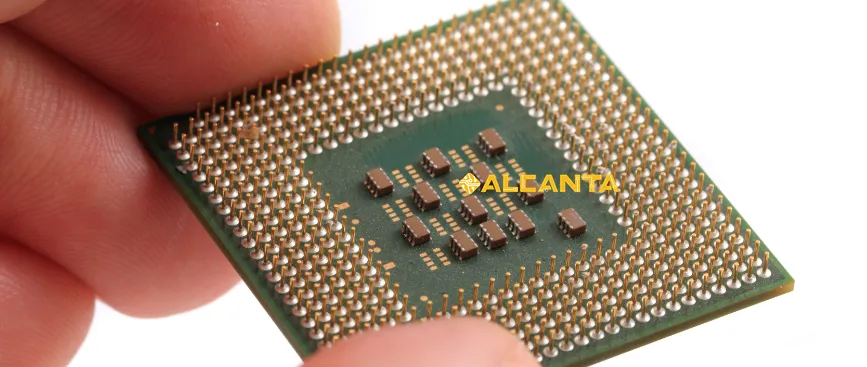
BGA Ball Composition
BGA balls, also known as solder balls, are essential components of BGA packages, serving as the primary means of electrical connection between the substrate and the circuit board. These small, spherical structures are typically composed of a lead-free solder alloy, such as tin-silver-copper (SnAgCu) or tin-bismuth (SnBi), chosen for its superior mechanical and thermal properties.
The manufacturing process of BGA balls involves several steps to ensure precise size, shape, and composition. Initially, the solder alloy is melted and formed into spherical shapes through a process called solder ball deposition. This can be achieved using various methods such as solder ball placement machines or solder ball reflow techniques. Once formed, the solder balls are carefully placed onto the substrate’s surface, typically through a solder paste or flux, and then heated to reflow temperature to attach them securely.
The role of BGA balls in the package assembly is paramount. During the assembly process, the solder balls serve as electrical interconnects, establishing connections between the contact pads on the substrate and the corresponding pads on the circuit board. Upon reflow, the solder balls melt and form reliable solder joints, ensuring secure electrical connections while also providing mechanical support to the package. Additionally, the spherical shape of the balls allows for slight misalignment between the substrate and the circuit board, accommodating for thermal expansion and contraction during operation.
In summary, BGA balls play a critical role in BGA package assembly by providing reliable electrical connections between the substrate and the circuit board. Their carefully engineered composition and manufacturing process ensure robust solder joints, contributing to the overall reliability and performance of electronic devices.
Components of BGA Package
Within a BGA package, several key components work in tandem to ensure its reliability and performance. Here’s a detailed exploration:
1. Substrate:
The substrate serves as the foundation of the BGA package, providing mechanical support and electrical connectivity between the semiconductor chip and the circuit board. It consists of layers of insulating material with conductive traces and vias to route signals and power.
2. Die:
The die, or semiconductor chip, is the heart of the BGA package, containing the integrated circuits (ICs) responsible for performing specific functions. The die is mounted onto the substrate and wire bonded to establish electrical connections between its bond pads and the substrate’s contact pads.
3. Wire Bonds:
Wire bonds are thin wires made of gold or aluminum that connect the bond pads on the die to the contact pads on the substrate. These wire bonds provide electrical pathways for signals to flow between the die and the substrate.
4. Encapsulant:
The encapsulant, often made of epoxy resin, surrounds the die and wire bonds, providing protection from external contaminants, moisture, and mechanical stress. It also serves to enhance the mechanical stability of the package and improve thermal dissipation.
5. Lid:
In some BGA packages, a lid or cover is placed over the die and encapsulant to further protect the components from environmental hazards and mechanical damage. The lid may also aid in heat dissipation by providing a path for heat to escape from the package.
Functionality and Importance:
– The substrate is crucial for providing electrical connectivity between the die and the circuit board, as well as supporting the mechanical integrity of the package.
– The die houses the electronic components and is responsible for the package’s primary function. Its proper integration onto the substrate ensures optimal performance.
– Wire bonds establish electrical connections between the die and the substrate, enabling the transmission of signals and power.
– The encapsulant protects the delicate components from external factors, ensuring the reliability and longevity of the package.
– The lid adds an additional layer of protection and can aid in thermal management, contributing to the overall reliability and performance of the BGA package.
In conclusion, each component within a BGA package plays a vital role in ensuring its reliability and performance. Through careful design and integration, these components work together to create robust and efficient electronic devices.
Standard BGA Size
Standard BGA sizes vary depending on the specific application and industry requirements. However, some common BGA package sizes are widely used across various industries due to their versatility and compatibility with standard assembly processes. These include:
1. 1.0 mm Pitch BGA: This BGA size features a ball pitch (spacing between the centers of adjacent solder balls) of 1.0 mm. It is commonly used in consumer electronics such as smartphones, tablets, and digital cameras, where space constraints are critical.
2. 0.8 mm Pitch BGA: With a smaller ball pitch of 0.8 mm, this BGA size offers higher I/O density and is suitable for applications requiring increased functionality in a compact form factor. It finds applications in networking equipment, automotive electronics, and industrial control systems.
3. 0.65 mm Pitch BGA: This BGA size is characterized by a tighter ball pitch of 0.65 mm, enabling even higher I/O counts and finer routing capabilities. It is commonly used in high-performance computing, telecommunications infrastructure, and aerospace applications.
4. 0.5 mm Pitch BGA: Featuring a ball pitch of 0.5 mm, this BGA size offers exceptional I/O density and is suitable for advanced electronic devices such as high-end servers, graphics processors, and FPGA (Field-Programmable Gate Array) devices.
Industry standards and guidelines play a crucial role in ensuring interoperability and compatibility between BGA packages from different manufacturers. Organizations such as the Joint Electron Device Engineering Council (JEDEC) and the International Electrotechnical Commission (IEC) establish standards and specifications for BGA package dimensions, materials, and reliability testing.
These standards define parameters such as ball pitch, ball diameter, package thickness, and overall package dimensions to ensure consistency and reliability across different BGA packages. Compliance with industry standards helps manufacturers design and produce BGA packages that meet the requirements of diverse applications and adhere to quality and reliability standards.
In summary, standard BGA sizes cater to a wide range of applications across industries, offering versatility, compactness, and high performance. Industry standards and guidelines ensure consistency, compatibility, and reliability in BGA package design and manufacturing processes, fostering innovation and interoperability in the electronics industry.
FAQs about bga substrate cross section
The substrate in BGA (Ball Grid Array) serves as the foundation of the package assembly, providing mechanical support and electrical connectivity between the semiconductor chip and the circuit board.
BGA balls, also known as solder balls, are typically made of a lead-free solder alloy, such as tin-silver-copper (SnAgCu) or tin-bismuth (SnBi), chosen for its mechanical and thermal properties.
The components of a BGA package include the substrate, die (semiconductor chip), wire bonds, encapsulant, and optionally a lid or cover.
The standard BGA size can vary depending on the specific application and industry requirements. Common BGA package sizes include 1.0 mm pitch, 0.8 mm pitch, 0.65 mm pitch, and 0.5 mm pitch, each offering different levels of I/O density and suitability for various electronic devices and applications.

