
Small Outline Integrated Circuit(SOIC) in PCB Design
The Small Outline Integrated Circuit (SOIC) is a widely used surface-mount IC package that offers reduced size, improved thermal performance, and enhanced electrical characteristics compared to traditional through-hole components. Its compact and standardized form factor makes it ideal for both consumer and industrial electronics. In modern electronics, the SOIC plays a crucial role in miniaturization, enabling the design of smaller, lightweight devices. Its compatibility with automated soldering processes ensures cost-effectiveness and reliability in high-volume production. Extensively used in PCB design, the SOIC is found in applications like microcontrollers, memory chips, and analog circuits, particularly in automotive electronics, communication systems, and medical devices, where space-saving and high-performance integration are essential.
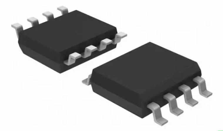
What is Small Outline Integrated Circuit (SOIC)?
The Small Outline Integrated Circuit (SOIC) is a type of surface-mount integrated circuit package known for its compact, rectangular design with gull-wing leads extending from its sides. It is widely used in modern electronics due to its space-efficient structure and compatibility with automated assembly processes. SOIC typically comes in two standard widths—narrow body (3.9mm) and wide body (7.5mm)—with varying pin counts depending on the specific application.
Compared to other IC packaging types such as Dual In-line Package (DIP) and Quad Flat Package (QFP), this package offers a significant reduction in size while maintaining ease of handling and soldering. Unlike DIP, which requires through-hole mounting, this package is designed for surface mounting, eliminating the need for drilled holes in the PCB. Additionally, compared to QFP, which has leads on all four sides, it has leads only on two sides, making it easier to inspect and solder.
In PCB assembly, the Small Outline Integrated Circuit (SOIC) plays a crucial role in reducing board space while maintaining high electrical performance. Its surface-mount nature allows for automated pick-and-place assembly, increasing production efficiency. Furthermore, SOIC’s gull-wing leads provide strong solder joints and reliable electrical connections, making it a preferred choice for applications such as microcontrollers, memory chips, and power management ICs in consumer electronics, automotive systems, and industrial equipment.
SOIC Package Dimensions and Variants of Small Outline Integrated Circuit (SOIC)
The Small Outline Integrated Circuit (SOIC) comes in various dimensions to accommodate different applications, with standardized widths, pin pitches, and heights. Typically, the package width is classified into two main categories: narrow-body and wide-body. It features a pin pitch of 1.27mm, ensuring reliable soldering and electrical performance. The package height generally ranges from 1.5mm to 2.65mm, making it a compact solution for surface-mount applications.
Comparison of Narrow-Body vs. Wide-Body SOIC Packages
The package is available in two common width variations:
- Narrow-body SOIC (JEDEC MS-012): Has a width of approximately 3.9mm and is commonly used for lower pin-count configurations (8 to 16 pins). It is ideal for compact PCB designs where board space is a constraint.
- Wide-body SOIC (JEDEC MS-013): Features a larger width of 7.5mm, allowing for higher pin counts (typically 16 to 28 pins). The increased width provides better heat dissipation and electrical performance, making it suitable for power management ICs and complex circuits.
Common Pin Counts and Their Applications
The SOIC is available in multiple pin configurations, each tailored to specific electronic applications:
- SOIC-8: Commonly used for operational amplifiers, EEPROMs, and small microcontrollers.
- SOIC-14 to SOIC-16: Found in logic ICs, communication interfaces, and low-power microcontrollers.
- SOIC-20 to SOIC-28: Utilized in higher-performance microcontrollers, voltage regulators, and memory ICs.
- SOIC-32 and above: Used in complex applications, including high-speed data processing and power management circuits.
The standardized form factors of the Small Outline Integrated Circuit (SOIC) enable seamless integration into modern PCB designs, balancing space efficiency, electrical performance, and ease of manufacturing.
SOIC vs. Other IC Packages: Comparing Small Outline Integrated Circuit (SOIC) with Alternatives
The Small Outline Integrated Circuit (SOIC) is one of the most commonly used surface-mount IC packages, but it is not the only option available. Depending on the application, designers may choose alternative packages such as TSSOP, QFP, SOT, or even SoC. Each package type has distinct characteristics that affect its suitability for different circuits and PCB layouts. Below is a detailed comparison of SOIC with these alternatives.
SOIC vs. TSSOP (Thin Shrink Small Outline Package)
Both the SOIC and TSSOP are surface-mount packages, but they differ in size and pin pitch:
- Size: TSSOP is a thinner and more compact version of SOIC, designed for applications where board space is limited. While a standard SOIC has a height of around 1.5–2.65mm, TSSOP is much thinner, typically below 1.2mm.
- Pin Pitch: TSSOP has a smaller pin pitch (0.65mm or even 0.5mm), whereas SOIC uses a standard 1.27mm pitch, making SOIC easier to solder and inspect.
- Application: TSSOP is preferred in high-density PCB layouts, such as memory ICs and power management circuits, while SOIC is chosen for applications requiring easier handling and better mechanical reliability.
SOIC vs. QFP (Quad Flat Package)
QFP (Quad Flat Package) is another widely used surface-mount package, but it has a different lead arrangement compared to Small Outline Integrated Circuit (SOIC):
- Lead Configuration: The SOIC has leads on only two sides of the package, while QFP has leads on all four sides. This makes QFP more suitable for high-pin-count ICs.
- Size and Complexity: QFP packages are generally larger and have finer lead pitches, often requiring more precise soldering techniques. In contrast, the SOIC is easier to work with, making it ideal for simpler circuit designs.
- Application: QFP is commonly used in microprocessors and high-performance ICs, whereas the SOIC is widely used in analog ICs, memory chips, and low-to-medium pin-count microcontrollers.
SOIC vs. SOT (Small Outline Transistor Package)
SOT (Small Outline Transistor) is designed primarily for discrete components such as transistors and diodes, making it significantly different from the Small Outline Integrated Circuit (SOIC):
- Component Type: The SOIC is used for multi-pin ICs, while SOT is mainly for single transistors, voltage regulators, and MOSFETs.
- Pin Count: SOT packages typically have 3–6 pins, while the SOIC can accommodate 8 to 32 pins or more.
- Application: SOT is ideal for power management and signal amplification in compact circuits, while the SOIC is used in more complex digital and analog circuits requiring multiple connections.
SOIC vs. SoC (System on Chip) – Understanding the Differences
A Small Outline Integrated Circuit (SOIC) is a physical packaging format, whereas SoC (System on Chip) refers to a highly integrated circuit that combines multiple functionalities:
- Scope: The SOIC is a standalone package used for discrete ICs, while an SoC integrates a processor, memory, and peripherals onto a single chip.
- Complexity: SoCs are much more advanced, often used in smartphones, embedded systems, and AI applications, whereas the SOIC is commonly found in simpler, modular designs.
- Application: While an SoC is used in high-performance computing and embedded systems, the SOIC remains a staple in traditional electronic components, such as amplifiers, memory, and logic circuits.
The SOIC remains a popular choice due to its balance between size, ease of manufacturing, and reliability. However, depending on the specific application, alternative packages like TSSOP, QFP, SOT, or SoC may be better suited for certain designs.
Advantages and Disadvantages of Small Outline Integrated Circuit (SOIC)
The Small Outline Integrated Circuit (SOIC) is a widely used surface-mount package that strikes a balance between compact size, ease of manufacturing, and reliable performance. It is preferred in many electronic applications due to its space efficiency and compatibility with automated assembly processes. However, like any other package type, SOIC has certain limitations, particularly in high-density and thermally demanding applications. Below is a detailed look at its advantages and disadvantages.
Advantages of Small Outline Integrated Circuit (SOIC)
Space-Efficient Design
One of the biggest advantages of the Small Outline Integrated Circuit (SOIC) is its compact size. Compared to traditional Dual In-line Package (DIP) components, SOIC reduces the required PCB footprint by approximately 30–50%, making it an ideal choice for modern electronics where board space is a crucial factor. This allows designers to create smaller and more portable devices without compromising functionality.
Suitable for Automated PCB Assembly
The SOIC is designed for surface-mount technology (SMT), which makes it compatible with automated pick-and-place machines. This automation increases production efficiency, reduces labor costs, and minimizes human errors in soldering. Additionally, the gull-wing leads of SOIC facilitate easy inspection and rework, further enhancing the reliability of mass production.
Reliable Electrical Performance
The Small Outline Integrated Circuit (SOIC) provides better electrical performance compared to through-hole packages like DIP. Its shorter leads help reduce parasitic inductance and capacitance, which is particularly beneficial for high-frequency applications. This improved signal integrity makes SOIC a suitable choice for analog circuits, microcontrollers, and memory chips used in various electronic devices.
Disadvantages of Small Outline Integrated Circuit (SOIC)
Not Ideal for High-Density Applications Compared to Smaller Packages
Although the Small Outline Integrated Circuit (SOIC) is smaller than DIP, it is not the most compact surface-mount package available. Newer, more advanced packages such as Thin Shrink Small Outline Package (TSSOP), Quad Flat No-Lead (QFN), and Ball Grid Array (BGA) provide even greater space savings. In applications where ultra-miniaturization is required, such as smartphones and wearable devices, designers often opt for these smaller alternatives instead of SOIC.
Limited Thermal Performance
The SOIC has limitations in terms of heat dissipation. Compared to larger packages with exposed thermal pads or heat sinks, SOIC’s ability to dissipate heat is relatively weaker. This can pose challenges in high-power applications where heat management is critical. Without proper PCB design techniques such as thermal vias or external heat sinks, excessive heat buildup in SOIC components could lead to performance degradation or failure over time.
The Small Outline Integrated Circuit (SOIC) remains a popular choice in PCB design due to its balance of size, cost-effectiveness, and ease of manufacturing. It is well-suited for medium-density applications requiring reliable electrical performance and automated assembly. However, for high-density circuit layouts or thermally demanding environments, alternative packaging solutions may be more appropriate. By understanding the strengths and limitations of SOIC, engineers can make informed decisions when selecting IC packages for their designs.

