
Navigating Flip Chip Packages: Efficiency at its Core
Flip chip packaging, a cutting-edge technology in semiconductor assembly, involves directly mounting the chip onto the substrate, flipping it upside down. This method enables compact designs, enhances electrical performance, and optimizes thermal management. In today’s electronics landscape, characterized by a relentless pursuit of smaller, faster, and more powerful devices, flip chip packaging has emerged as a pivotal solution. Its importance lies in its ability to meet the demands of miniaturization while ensuring superior performance and reliability. As industries push the boundaries of innovation, flip chip packaging has become indispensable, driving advancements in smartphones, IoT devices, autonomous vehicles, and beyond. Understanding its principles and applications is essential for engineers and enthusiasts alike, as it continues to shape the future of modern electronics.
Overview of Flip Chip Packaging
Definition and Working Principle
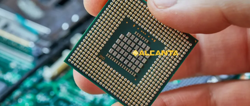
Flip chip packaging is an advanced semiconductor assembly technique where the integrated circuit (IC) chip is directly mounted onto a substrate with its active side facing downwards. This method allows for a more compact and efficient layout compared to traditional packaging methods like wire bonding. The working principle involves the use of small solder bumps, known as Controlled Collapse Chip Connection (C4) bumps, which serve as electrical connections between the chip and the substrate. These bumps are carefully aligned and soldered to corresponding pads on the substrate, forming a direct electrical connection.
Comparison with Other Packaging Technologies
When compared to other packaging technologies such as IC package, Land Grid Array (LGA) package, and Dual in-line package (DIP), flip chip packaging offers several distinct advantages. Unlike IC packaging, which typically involves encapsulating the chip within a protective casing, flip chip packaging exposes the active side of the chip, facilitating better thermal dissipation and electrical performance. Compared to LGA and DIP packages, flip chip packaging enables higher interconnect densities and shorter signal paths, resulting in improved signal integrity and faster data transmission.
Introduction to Basic Concepts
Key concepts in flip chip packaging include the C4 bump and the semiconductor chip itself. C4 bumps are small solder bumps made of a lead-free alloy, typically composed of tin and silver. These bumps serve as the electrical and mechanical connections between the chip and the substrate. The semiconductor chip, often made of silicon, contains the integrated circuitry and is the core component of the flip chip package. Understanding these fundamental elements is crucial for grasping the intricacies of flip chip packaging technology.
Advantages of Flip Chip Packaging
1. Reduction in Package Size: Flip chip packaging offers a significant reduction in package size compared to traditional packaging methods. By directly mounting the chip onto the substrate, flip chip technology eliminates the need for wire bonding and external packaging materials. This results in a more compact footprint, making it ideal for applications where space is limited, such as mobile devices, wearables, and IoT sensors.
2. Enhanced Electrical Performance: The direct connection between the semiconductor chip and the substrate in flip chip packaging results in shorter interconnect lengths and reduced parasitic capacitance and inductance. This leads to enhanced electrical performance, including faster signal propagation, lower signal loss, and improved signal integrity. As a result, flip chip packages are well-suited for high-speed data transmission and high-frequency applications.
3. Improved Thermal Management: Flip chip packaging offers superior thermal management compared to traditional packaging methods. With the active side of the chip facing downwards and in direct contact with the substrate, heat dissipation is more efficient. This allows for better thermal conductivity and heat dissipation, reducing the risk of overheating and improving the overall reliability and longevity of the semiconductor device.
4. Increased Reliability: The elimination of wire bonds in flip chip packaging reduces the risk of wire bond failures, which are common sources of reliability issues in traditional packaging methods. Additionally, flip chip packages have fewer mechanical stress points, resulting in improved resistance to mechanical shock, vibration, and thermal cycling. This increased reliability makes flip chip technology particularly suitable for demanding applications in automotive, aerospace, and industrial environments.
5. Other Advantages:
- Higher interconnect density: Flip chip packaging allows for a higher density of interconnects compared to traditional packaging methods, enabling more complex designs and functionalities.
- Better electrical performance at high frequencies: The shorter interconnect lengths and reduced parasitic effects in flip chip packaging result in improved electrical performance, particularly at high frequencies.
- Compatibility with advanced packaging technologies: Flip chip packaging is compatible with various advanced packaging techniques, such as Through-Silicon Via (TSV) technology and wafer-level packaging, enabling further miniaturization and integration of semiconductor devices.
Applications of Flip Chip Packaging
1. Chip Scale Package (CSP): Flip chip packaging is widely used in Chip Scale Package (CSP) configurations, where the package size closely matches the dimensions of the semiconductor chip itself. CSPs offer a high level of miniaturization and are commonly employed in compact electronic devices such as smartphones, tablets, smartwatches, and other portable consumer electronics. The small form factor and efficient thermal management of flip chip CSPs make them ideal for applications where space is at a premium.
2. Chip on Board (COB): Flip chip packaging is also utilized in Chip on Board (COB) configurations, where the semiconductor chip is directly mounted onto a printed circuit board (PCB) without the use of an additional package. COB assemblies are commonly found in LED lighting modules, where flip chip LEDs are directly bonded to the PCB substrate. COB technology offers advantages such as improved thermal management, simplified assembly processes, and reduced form factor, making it suitable for various lighting applications.
3. Overview of Application Areas:
- Telecommunications: In telecommunications, flip chip packaging is used in networking equipment, routers, switches, and optical transceivers. The compact size, high-speed performance, and reliability of flip chip packages make them well-suited for high-bandwidth communication systems and data centers.
- Computing: In computing devices such as laptops, desktops, servers, and data storage systems, flip chip packaging enables high-performance processors, memory modules, and graphics processing units (GPUs) to be densely packed and efficiently cooled. This enhances computing power while maintaining a compact form factor.
- Automotive: In automotive electronics, flip chip packaging is utilized in advanced driver-assistance systems (ADAS), infotainment systems, engine control units (ECUs), and sensors. Flip chip packages offer robustness, reliability, and resistance to harsh operating conditions such as temperature variations, vibrations, and humidity, making them essential for automotive applications.
- Medical: In the medical field, flip chip packaging is employed in implantable medical devices, diagnostic equipment, and wearable health monitors. The small size, low power consumption, and high reliability of flip chip packages enable the development of innovative medical devices that can monitor, diagnose, and treat various medical conditions with precision and efficiency.
Overall, the versatility, performance, and reliability of flip chip packaging make it indispensable across a wide range of industries and applications, driving advancements in technology and enabling the development of innovative electronic devices.
Flip Chip Packaging Technology
Overview of Packaging Process: Flip chip packaging involves several key steps to assemble the semiconductor chip onto the substrate. The process typically includes die preparation, bumping, wafer thinning (if necessary), die bonding, underfilling (optional), and testing. Each step plays a crucial role in ensuring the reliability and performance of the flip chip package.
Evolution of Technology: Flip chip packaging has evolved significantly over the years, driven by advancements in materials, equipment, and manufacturing processes. Early flip chip technologies relied on wire bonding and gold bumping techniques. However, with the development of solder bumping methods such as Controlled Collapse Chip Connection (C4), flip chip packaging has become more cost-effective, reliable, and scalable. Recent innovations include the integration of Through-Silicon Via (TSV) technology, which enables vertical interconnects within the semiconductor chip, further enhancing performance and miniaturization.
Detailed Explanation of Packaging Steps
- Die Preparation: The semiconductor wafer undergoes various processes such as dicing, cleaning, and inspection to prepare individual chips.
- Bumping: Solder bumps are deposited onto the bonding pads of the semiconductor chip using methods such as electroplating or solder jetting.
- Wafer Thinning: In some cases, the semiconductor wafer may be thinned to reduce thickness and improve electrical performance.
- Die Bonding: The semiconductor chip is precisely aligned and bonded onto the substrate using adhesive materials or solder reflow processes.
- Underfilling (Optional): An underfill material may be dispensed between the chip and substrate to improve mechanical strength and reliability.
- Testing: The assembled flip chip package undergoes electrical and functional testing to ensure proper functionality.
Key Process Parameters
- Alignment Accuracy: Precise alignment of the semiconductor chip with the substrate is critical for ensuring electrical connectivity and reliability.
- Bump Pitch and Size: The pitch and size of the solder bumps determine the density of interconnects and overall package size.
- Solder Reflow Profile: The temperature and time profile during solder reflow processes affect the quality of solder joints and overall package reliability.
- Underfill Material Properties: The properties of underfill materials, such as viscosity, curing time, and coefficient of thermal expansion (CTE), impact package reliability and thermal performance.
Equipment and Materials Involved: Equipment used in flip chip packaging includes die bonders, solder bumping machines, reflow ovens, and inspection tools. Materials commonly used in flip chip packaging include solder alloys for bumping, adhesive materials for die bonding, underfill materials, and substrate materials such as organic laminate or ceramic substrates. Advances in equipment and materials continue to drive improvements in flip chip packaging technology, enabling higher performance, reliability, and scalability.
Flip Chip Packaging Tutorial
Beginner’s Guide: Before diving into the flip chip packaging process, it’s essential to familiarize yourself with the basic concepts and terminology associated with this technology. This includes understanding the role of solder bumps, the importance of alignment accuracy, and the key steps involved in assembling a flip chip package.
Illustrated Packaging Process Flow: Below is an illustrated flowchart outlining the typical steps involved in flip chip packaging:
| Step | Description |
| 1. Die Preparation | Prepare semiconductor wafer and dice into individual chips. |
| 2. Bumping | Deposit solder bumps onto bonding pads of the chip. |
| 3. Die Bonding | Align and bond the chip onto the substrate. |
| 4. Underfilling | Optional step to dispense underfill material. |
| 5. Testing | Electrical and functional testing of the assembled package. |
Step-by-Step Operational Guide
- Die Preparation: Begin by dicing the semiconductor wafer into individual chips using a dicing saw. Ensure proper cleaning and inspection of the diced chips to remove any contaminants.
- Bumping: Deposit solder bumps onto the bonding pads of the semiconductor chip using electroplating or solder jetting techniques. Control the size, shape, and pitch of the solder bumps according to design specifications.
- Die Bonding: Align the solder-bumped semiconductor chip with the corresponding pads on the substrate. Use a die bonder to precisely position and bond the chip onto the substrate using adhesive materials or solder reflow processes.
- Underfilling (Optional): Dispense underfill material around the perimeter of the bonded chip to improve mechanical strength and reliability. Ensure proper curing of the underfill material according to manufacturer recommendations.
- Testing: Perform electrical and functional testing of the assembled flip chip package to verify proper connectivity and functionality. Use automated test equipment (ATE) to conduct tests such as continuity, impedance, and functionality tests.
FAQs About Flip Chip Packaging
Flip chip packaging offers advantages such as reduced package size, enhanced electrical performance, improved thermal management, and increased reliability compared to wire bonding.
Important design considerations include bump pitch and size, substrate material selection, thermal management, and alignment accuracy.
Proper alignment can be achieved using advanced alignment systems in die bonders, which utilize vision systems and precision stages to align the chip with the substrate pads accurately.
Underfilling is optional but recommended for flip chip packages, especially in applications where mechanical robustness and reliability are critical. It helps to mitigate stresses caused by thermal cycling and mechanical shock.
Flip chip packaging is an advanced semiconductor assembly technique where the semiconductor chip is directly mounted onto a substrate, such as a printed circuit board (PCB) or ceramic substrate, with its active side facing downwards. This method eliminates the need for wire bonding by using small solder bumps, known as Controlled Collapse Chip Connection (C4) bumps, to establish electrical connections between the chip and the substrate. Flip chip packaging offers advantages in terms of miniaturization, performance, and reliability compared to traditional packaging methods.
Flip chip packaging falls under the category of chip-scale packages (CSPs). CSPs are semiconductor packages designed to have dimensions that closely match those of the semiconductor chip itself. In flip chip packaging, the package size is minimized by directly mounting the chip onto the substrate, resulting in a compact and efficient package.
The main advantage of a flip chip package is its ability to offer superior electrical performance, miniaturization, and thermal management compared to traditional packaging methods like wire bonding. By eliminating the need for wire bonds and encapsulating the chip within a protective casing, flip chip packaging reduces interconnect lengths, parasitic capacitance, and inductance, resulting in improved signal integrity and faster data transmission. Additionally, flip chip packages allow for better thermal dissipation, making them suitable for high-power and high-frequency applications.
A flip chip device refers to an electronic component or semiconductor chip that has been assembled using flip chip packaging technology. In a flip chip device, the semiconductor chip is mounted upside down onto a substrate, allowing for direct electrical connections between the chip and the substrate. Flip chip devices are commonly used in various electronic applications, including microprocessors, memory chips, sensors, and integrated circuits, where compact size, high performance, and reliability are essential.


发表评论
Want to join the discussion?Feel free to contribute!