
Revolutionizing Semiconductor Packaging: Advances in IC Package Substrate Material
In the realm of semiconductor packaging, IC package substrate materials play a pivotal role, serving as the backbone that supports and interconnects integrated circuits (ICs) within electronic devices. These substrates are not merely structural components but critical facilitators of electrical connectivity and thermal management. They provide the foundation for ICs to function reliably and efficiently in various applications, ranging from consumer electronics to industrial machinery. By bridging the gap between ICs and external components, substrate materials ensure seamless communication and power distribution within electronic systems. Understanding the significance of IC package substrate materials is fundamental to appreciating their contribution to the reliability, performance, and miniaturization of modern electronic devices.
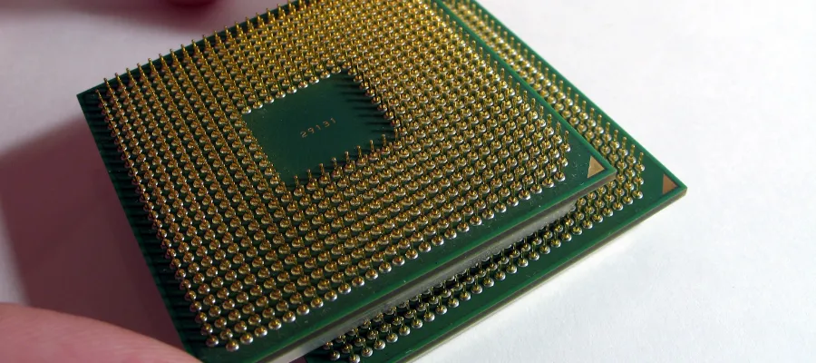
What is IC Substrate?
Definition of IC Substrate and its Significance in Semiconductor Packaging
An IC substrate, also known as a chip carrier or package substrate, is a specialized component in semiconductor packaging responsible for supporting and interconnecting integrated circuits (ICs) within electronic devices. It serves as a platform upon which IC chips are mounted, providing structural support and electrical connectivity. The substrate’s significance lies in its role as a crucial intermediary between the IC chips and the rest of the electronic system, facilitating signal transmission, power distribution, and thermal dissipation.
Differentiation between IC Substrate and PCB (Printed Circuit Board)
While both IC substrates and printed circuit boards (PCBs) are essential elements in electronic devices, they serve distinct purposes. PCBs are primarily used for connecting and supporting various electronic components, including ICs, resistors, and capacitors, to form a complete electronic circuit. In contrast, IC substrates are specifically designed to support IC chips, providing a more focused and specialized function within semiconductor packaging. Additionally, IC substrates often feature finer traces and more complex layouts tailored to accommodate the specific requirements of ICs.
Overview of the Functions and Features of IC Substrates
IC substrates perform several critical functions essential for the operation and performance of semiconductor devices:
- Electrical Connectivity: IC substrates feature intricate wiring patterns that enable electrical connections between the IC chips and external components, ensuring proper signal transmission and power delivery.
- Thermal Management: The substrate’s material properties and design contribute to efficient heat dissipation, helping to regulate the temperature of the ICs and prevent overheating, which can degrade performance and reliability.
- Mechanical Support: IC substrates provide structural support for the IC chips, protecting them from mechanical stress, shock, and vibration during operation and handling.
- Miniaturization and Integration: Advanced substrate technologies enable the integration of multiple ICs and passive components into compact packages, contributing to the miniaturization and high-density packaging of electronic devices.
- Signal Integrity: Careful design and layout considerations in IC substrates help maintain signal integrity by minimizing impedance mismatches, crosstalk, and other electrical anomalies that could affect the performance of the ICs and the overall system.
Overall, IC substrates play a vital role in semiconductor packaging, enabling the reliable operation, performance, and miniaturization of modern electronic devices across a wide range of applications.
IC Substrate Material Suppliers
Exploration of Major Suppliers Providing IC Substrate Materials in the Semiconductor Industry
In the semiconductor industry, several key players specialize in supplying IC substrate materials to manufacturers worldwide. These suppliers offer a wide range of materials tailored to meet the diverse requirements of semiconductor packaging applications. Some of the prominent IC substrate material suppliers include:
- Amkor Technology: Amkor Technology is a leading provider of semiconductor packaging and test services, offering a comprehensive portfolio of IC substrate materials, including laminate substrates, leadframe-based substrates, and fan-out wafer-level packaging (FOWLP) solutions.
- Shinko Electric Industries Co., Ltd.: Shinko Electric Industries is a renowned manufacturer of semiconductor packaging substrates, including flip-chip substrates, high-density interconnect (HDI) substrates, and build-up substrates. The company’s advanced technologies cater to the evolving needs of the semiconductor industry.
- Unimicron Technology Corporation: Unimicron Technology Corporation specializes in the production of high-quality IC substrates, such as organic substrates, ceramic substrates, and IC carriers. The company’s advanced manufacturing facilities and stringent quality control measures ensure reliability and performance excellence.
- Kinsus Interconnect Technology Corp.: Kinsus Interconnect Technology Corp. is a leading provider of semiconductor packaging solutions, offering a diverse range of substrate materials, including laminate substrates, build-up substrates, and embedded substrate technologies. The company’s innovative products support the development of cutting-edge electronic devices.
- Taiyo Holdings Co., Ltd.: Taiyo Holdings Co., Ltd. is a global supplier of advanced substrate materials for semiconductor packaging applications. The company’s product portfolio encompasses IC substrates, build-up substrates, and thermal substrates, designed to meet the demanding requirements of next-generation electronic devices.
Discussion on the Criteria for Selecting Substrate Material Suppliers
When selecting substrate material suppliers for semiconductor packaging projects, manufacturers consider several critical criteria to ensure optimal performance, reliability, and cost-effectiveness. These criteria include:
- Material Quality: Suppliers must adhere to stringent quality standards to deliver materials with consistent performance and reliability. Manufacturers evaluate the supplier’s track record, certifications, and quality control processes to ensure the reliability of the substrate materials.
- Technological Expertise: Suppliers with expertise in advanced substrate technologies and manufacturing processes can offer innovative solutions to meet the evolving requirements of semiconductor packaging. Manufacturers assess the supplier’s R&D capabilities, technological advancements, and intellectual property portfolio to gauge their ability to deliver cutting-edge solutions.
- Supply Chain Stability: Suppliers with a robust supply chain and global manufacturing capabilities can ensure timely delivery of substrate materials to meet production schedules and market demands. Manufacturers evaluate the supplier’s supply chain resilience, production capacity, and geographic presence to mitigate supply chain risks.
- Cost Competitiveness: While quality and performance are paramount, manufacturers also consider the cost competitiveness of substrate material suppliers to maintain profitability and competitiveness in the market. Evaluating the supplier’s pricing structure, cost-efficiency initiatives, and value-added services can help manufacturers optimize their procurement decisions.
- Customer Support: Effective communication, technical support, and after-sales service are essential factors in selecting substrate material suppliers. Manufacturers assess the supplier’s responsiveness, collaboration capabilities, and willingness to provide customized solutions to address specific requirements and challenges.
By carefully evaluating these criteria, semiconductor manufacturers can select reliable substrate material suppliers that meet their technical, operational, and business objectives, ultimately contributing to the success of their semiconductor packaging projects.
IC Substrate Manufacturing Process
Detailed Explanation of the Manufacturing Process Involved in Producing IC Substrates
The manufacturing process of IC substrates involves several intricate steps aimed at fabricating high-quality substrates capable of supporting and interconnecting integrated circuits effectively. These steps typically include material selection, substrate fabrication, metallization, and testing. Let’s delve into each stage in detail:
1. Material Selection
- The manufacturing process begins with the selection of suitable substrate materials based on the specific requirements of the semiconductor packaging application.
- Common substrate materials include silicon, glass, ceramics, and organic materials like laminate and build-up substrates.
- Material properties such as thermal conductivity, electrical insulation, mechanical strength, and dimensional stability are carefully considered during the selection process to ensure optimal performance.
2. Substrate Fabrication
- The substrate fabrication process involves several key steps, including substrate preparation, patterning, and etching:
a. Substrate Preparation: The selected substrate material undergoes surface preparation treatments to ensure cleanliness and uniformity, essential for subsequent processing steps.
b. Patterning: A photoresist layer is applied to the substrate surface, followed by exposure to ultraviolet (UV) light through a photomask. This step defines the desired circuit pattern on the substrate surface.
c. Etching: The exposed areas of the substrate are etched using chemical or plasma processes, selectively removing material to create the desired circuit features and interconnects.
3. Metallization
- After patterning and etching, the substrate undergoes metallization to deposit conductive metal layers onto the circuit pattern.
- Techniques such as sputtering, evaporation, or electroplating are commonly used to deposit metal films such as copper, aluminum, or gold onto the substrate surface.
- The metallization process forms electrical interconnects, bonding pads, and routing traces necessary for connecting the integrated circuits to external components.
4. Testing
- Once metallization is complete, the fabricated IC substrates undergo rigorous testing to ensure adherence to quality and performance standards.
- Testing methods may include electrical continuity tests, impedance measurements, thermal cycling tests, and visual inspections.
- Defective substrates are identified and either repaired or discarded to maintain product quality and reliability.
IC substrate manufacturing utilizes a variety of materials, each with distinct properties and advantages suited to specific packaging requirements. Silicon, glass, ceramics, and organic materials like laminate and build-up substrates offer a diverse range of options for semiconductor packaging, enabling manufacturers to achieve optimal performance, reliability, and cost-effectiveness in electronic devices across various industries. Understanding the properties and advantages of each material type is essential for selecting the most suitable substrate for a given application.
Semiconductor Package Substrate
Examination of the Substrate’s Role within Semiconductor Packages
The substrate plays a critical role within semiconductor packages, serving as the foundation upon which integrated circuits (ICs) are mounted and interconnected. It provides structural support, electrical connectivity, and thermal management for the ICs, facilitating their integration into electronic devices. The substrate acts as a bridge between the ICs and the rest of the package components, enabling efficient communication, power distribution, and heat dissipation.
Discussion on How Substrate Materials Contribute to Thermal Management, Signal Integrity, and Electrical Connectivity
- Thermal Management
- Substrate materials with high thermal conductivity, such as ceramics and certain types of organic materials, help dissipate heat generated by the ICs during operation. By efficiently conducting heat away from the ICs, the substrate prevents thermal buildup and ensures the reliable performance of electronic devices.
- Additionally, the substrate’s design, including the layout of thermal vias and heat spreaders, enhances thermal dissipation and regulates the temperature of the ICs within acceptable limits.
- Signal Integrity
- The substrate material’s dielectric properties and electrical characteristics significantly influence signal integrity within semiconductor packages. Low-loss materials with controlled dielectric constant and minimal signal attenuation are essential for maintaining signal integrity and reducing signal reflections and noise.
- Proper substrate design, including controlled impedance traces and signal routing techniques, helps minimize signal distortion and impedance mismatch, ensuring reliable data transmission and signal integrity.
- Electrical Connectivity
- Substrate materials, particularly metals used for interconnects and bonding pads, play a crucial role in facilitating electrical connectivity within semiconductor packages. Materials with high conductivity, such as copper and gold, are preferred for achieving low resistance and efficient power distribution.
- The substrate’s metallization process, including deposition techniques and metallization thickness, influences the electrical performance and reliability of interconnects, bonding wires, and solder joints.
The substrate serves as a vital component within semiconductor packages, contributing to thermal management, signal integrity, and electrical connectivity. By selecting appropriate substrate materials and optimizing substrate design, semiconductor manufacturers can enhance the performance, reliability, and functionality of electronic devices across various applications. Effective thermal management, signal integrity, and electrical connectivity are essential for achieving optimal performance and ensuring the longevity of semiconductor packages in demanding operating environments.
IC Substrate vs. PCB
Detailed Comparison between IC Substrates and PCBs
1. Design
- IC Substrates: IC substrates are specifically designed to support and interconnect integrated circuits (ICs) within semiconductor packages. They typically feature intricate wiring patterns, fine traces, and complex layouts tailored to accommodate the specific requirements of ICs, including high-density interconnects and precise signal routing.
- PCBs: Printed circuit boards (PCBs) are designed to support various electronic components, including ICs, resistors, capacitors, and connectors, to form complete electronic circuits. PCB designs may vary depending on the application, ranging from single-layer to multi-layer boards, with features such as vias, pads, and traces optimized for specific functionalities.
2. Functionality
- IC Substrates: The primary function of IC substrates is to provide structural support, electrical connectivity, and thermal management for ICs within semiconductor packages. They facilitate signal transmission, power distribution, and heat dissipation, ensuring the reliable operation and performance of ICs in electronic devices.
- PCBs: PCBs serve as platforms for assembling and connecting electronic components to form functional circuits. They provide electrical connections between components, support mechanical mounting, and facilitate signal routing. PCBs also offer flexibility for incorporating various components and peripherals to meet specific application requirements.
3. Application
- IC Substrates: IC substrates are predominantly used in semiconductor packaging applications, where they play a crucial role in integrating ICs into electronic devices such as smartphones, tablets, computers, and automotive electronics. They are essential for miniaturization, high-density packaging, and thermal management in advanced semiconductor devices.
- PCBs: PCBs are utilized in a wide range of electronic devices and systems across industries, including consumer electronics, telecommunications, aerospace, and medical devices. They serve as foundational components in devices such as smartphones, televisions, routers, medical equipment, and industrial control systems, providing the necessary connectivity and functionality.
C
While IC substrates and PCBs share similarities as essential components in electronic devices, they serve distinct purposes and exhibit differences in design, functionality, and application. IC substrates are specialized components tailored for semiconductor packaging, offering features optimized for supporting and connecting ICs within compact and high-performance packages. In contrast, PCBs serve as versatile platforms for assembling and interconnecting various electronic components to form functional circuits in a wide range of electronic devices and systems. Understanding the differences between IC substrates and PCBs is essential for selecting the appropriate technology to meet specific application requirements and performance criteria.
Semiconductor Packaging Types
Overview of Different Semiconductor Packaging Types
- Flip-Chip Packaging
- In flip-chip packaging, ICs are mounted face-down onto the substrate or carrier, allowing direct electrical connections between the IC’s bond pads and the substrate’s metal traces.
- This packaging type offers superior electrical performance, shorter signal paths, and higher interconnect density compared to traditional wire-bond packaging.
- Flip-chip packaging is commonly used in high-performance applications such as microprocessors, graphic processors, and memory modules.
- Wire-Bond Packaging
- Wire-bond packaging involves connecting ICs to the substrate using thin wire bonds made of gold, aluminum, or copper.
- Wire bonds are attached from the IC’s bond pads to corresponding pads on the substrate, forming electrical connections.
- This packaging type is widely used in a variety of electronic devices due to its simplicity, reliability, and cost-effectiveness.
- Ball Grid Array (BGA)
- BGA packaging features an array of solder balls arranged on the underside of the IC, which are soldered to corresponding pads on the substrate.
- BGA packages offer high interconnect density, excellent thermal performance, and mechanical robustness, making them suitable for applications requiring reliability and miniaturization.
- BGA packaging is commonly found in consumer electronics, telecommunications, and automotive electronics.
Explanation of How Substrate Materials Vary Across Packaging Types
- Flip-Chip Packaging
- In flip-chip packaging, substrates often use materials with high thermal conductivity and low coefficient of thermal expansion (CTE) to efficiently dissipate heat generated by the ICs.
- Common substrate materials for flip-chip packaging include silicon, glass, and ceramic-based materials, which offer excellent thermal management capabilities.
- Wire-Bond Packaging
- Substrate materials for wire-bond packaging vary depending on the application requirements and cost considerations.
- Organic materials such as laminates and build-up substrates are commonly used for wire-bond packaging due to their cost-effectiveness and ease of manufacturing.
- Ball Grid Array (BGA)
- BGA packages typically utilize substrates made of materials with good mechanical strength, thermal conductivity, and solderability.
- Ceramic substrates are often preferred for BGA packaging, as they offer superior thermal management and reliability compared to organic substrates.
Semiconductor packaging types, such as flip-chip, wire-bond, and ball grid array (BGA), each have unique characteristics and utilize different substrate materials tailored to their specific requirements. Understanding the variations in substrate materials across packaging types is crucial for selecting the most suitable packaging solution for a given application, ensuring optimal performance, reliability, and cost-effectiveness.
Future Trends and Developments
Insight into Emerging Trends and Innovations in IC Substrate Materials
- Advanced Packaging Technologies
- The semiconductor industry is witnessing a shift towards advanced packaging technologies such as fan-out wafer-level packaging (FOWLP), system-in-package (SiP), and 3D integration.
- These technologies require innovative substrate materials with enhanced thermal conductivity, electrical performance, and reliability to meet the demands of high-performance and high-density packaging.
- Integration of Advanced Materials
- Emerging trends include the integration of advanced materials such as organic-inorganic hybrid substrates, flexible substrates, and nanocomposite materials into IC packaging.
- These materials offer unique properties such as flexibility, lightweight, and improved thermal management, enabling the development of next-generation electronic devices with enhanced functionality and form factors.
- Embedded Substrate Technologies
- Embedded substrate technologies, such as embedded passive components (EPC) and embedded active components (EAC), are gaining traction for miniaturization and integration in semiconductor packaging.
- These technologies involve integrating passive and active components directly into the substrate, reducing the footprint and improving the performance of electronic devices.
Discussion on How Advancements in Material Science and Manufacturing Techniques are Shaping the Future of Semiconductor Packaging
- Material Science Innovations
- Advances in material science are leading to the development of novel substrate materials with superior properties such as higher thermal conductivity, lower dielectric loss, and improved mechanical strength.
- Nanomaterials, such as carbon nanotubes and graphene, are being explored for their potential to enhance thermal conductivity and electrical performance in IC substrates.
- Manufacturing Technique Advancements
- Novel manufacturing techniques such as additive manufacturing (3D printing), laser micromachining, and advanced lithography processes are revolutionizing the fabrication of IC substrates.
- These techniques enable the production of complex substrate structures with micron-level precision, allowing for the integration of fine-pitch interconnects and advanced features in semiconductor packaging.
- Integration of AI and Data Analytics
- The integration of artificial intelligence (AI) and data analytics into semiconductor packaging manufacturing processes enables predictive maintenance, process optimization, and quality control.
- AI-driven algorithms analyze production data in real-time, identifying potential defects, optimizing process parameters, and improving yield rates in IC substrate fabrication.
C
The future of semiconductor packaging is shaped by ongoing advancements in material science, manufacturing techniques, and packaging technologies. Emerging trends such as advanced packaging technologies, integration of advanced materials, and embedded substrate technologies are driving innovation in IC substrate materials. Advancements in material science and manufacturing techniques are enabling the development of substrate materials with superior properties, while the integration of AI and data analytics is revolutionizing semiconductor packaging manufacturing processes. These developments are poised to unlock new possibilities in electronic device design, performance, and functionality, paving the way for the next generation of semiconductor packaging solutions.
FAQs About IC Package Substrate Materials
Package substrates can be made of various materials such as silicon, glass, ceramics, and organic materials like laminate and build-up substrates.
The substrate material for packaging can vary, but common options include silicon, glass, ceramics, and organic materials like laminate and build-up substrates.
The substrate of an IC (integrated circuit) can be made of various materials, including silicon, glass, ceramics, and organic materials such as laminate and build-up substrates.
The substrate of ICs refers to the material on which the integrated circuits are mounted and interconnected. It can be composed of silicon, glass, ceramics, or organic materials such as laminate and build-up substrates.


发表评论
Want to join the discussion?Feel free to contribute!