
Empowering Electronics with BT Package Substrate
The BT package substrate plays a pivotal role in modern electronics, serving as the foundation for intricate circuitry in various devices. Its importance lies in providing a robust platform for mounting and interconnecting electronic components, ensuring reliability and performance. From consumer electronics to aerospace applications, BT substrates find wide-ranging use due to their excellent thermal stability, electrical properties, and mechanical strength.
In this article, we aim to delve into the intricacies of BT package substrates, exploring their materials, manufacturing processes, and comparative analysis with other substrates like ABF. Furthermore, we will examine the differences between PCBs and package substrates, offering insights into their respective roles in electronic systems. Through case studies and analysis, we aim to provide a comprehensive understanding of BT package substrates, their applications, and their significance in the realm of modern electronics.
BT Substrate Material
Characteristics and Uses of BT Epoxy
BT epoxy, a key component of BT substrate material, is a type of epoxy resin renowned for its high thermal conductivity, excellent adhesion properties, and superior electrical insulation. It possesses exceptional heat resistance, making it suitable for applications requiring exposure to elevated temperatures, such as automotive electronics and industrial equipment. Additionally, BT epoxy exhibits low outgassing characteristics, making it ideal for use in high-vacuum environments, such as aerospace and satellite applications. Its compatibility with various fillers and reinforcement materials further enhances its mechanical properties, ensuring reliability in harsh operating conditions.
Features and Advantages of Mitsubishi BT Laminate
Mitsubishi BT laminate is a specialized type of substrate material engineered by Mitsubishi Electric Corporation. It offers a unique combination of properties, including high dielectric strength, low thermal expansion coefficient, and excellent dimensional stability. These features make Mitsubishi BT laminate well-suited for applications requiring precise signal integrity and thermal management, such as high-speed digital communication systems and power electronics. Its uniformity and consistency ensure predictable performance across different manufacturing batches, contributing to overall product reliability.
Role and Characteristics of Bismaleimide-Triazine Resin
Bismaleimide-triazine (BT) resin is a high-performance thermosetting polymer widely used in the fabrication of advanced electronic substrates. It exhibits outstanding thermal stability, flame resistance, and mechanical strength, making it suitable for demanding applications in aerospace, defense, and telecommunications industries. BT resin provides excellent adhesion to copper foils and substrate materials, ensuring reliable interconnection and signal transmission. Its inherent chemical resistance and low moisture absorption enhance the durability and long-term reliability of electronic assemblies.
Properties and Applications of ABF Substrate
Anisotropic Conductive Film (ACF) Bonding Films are advanced materials used in the fabrication of flexible printed circuits (FPC) and printed circuit boards (PCB). They consist of a base film, typically made of polyimide or polyester, coated with conductive particles on one or both sides. These films enable electrical connections between electronic components through a controlled heating and pressure process, forming reliable interconnects without the need for soldering. ACF bonding films offer numerous advantages, including flexibility, lightweight, and compatibility with fine-pitch components, making them ideal for applications requiring compact and lightweight electronic assemblies, such as wearable devices, mobile phones, and medical devices.
Process of BT Substrate
Material Preparation Stage
- Selection of BT epoxy, Mitsubishi BT laminate, and Bismaleimide-Triazine resin based on design requirements and performance specifications.
- Precise measurement and mixing of epoxy resin with hardeners and additives to achieve desired material properties.
- Preparation of Mitsubishi BT laminate sheets by cutting them to required dimensions and cleaning them to ensure surface cleanliness.
- Preparation of Bismaleimide-Triazine resin in accordance with manufacturer’s instructions, including temperature and viscosity control.
Printing and Stacking of Laminates
- Application of BT epoxy onto Mitsubishi BT laminate sheets using screen printing or roller coating techniques.
- Precise alignment and stacking of multiple coated laminate sheets to form a multi-layered substrate structure.
- Insertion of copper foil layers between BT epoxy-coated laminate sheets to create conductive pathways and signal traces.
- Application of pressure to ensure proper adhesion and consolidation of the laminate stack.
Thermal Compression and Curing Process
- Transfer of the assembled laminate stack to a heated press or vacuum chamber for thermal compression.
- Application of controlled temperature and pressure to promote the flow and curing of the BT epoxy resin.
- Monitoring of key process parameters such as temperature, pressure, and curing time to ensure uniformity and consistency.
- Cooling of the cured laminate stack to room temperature to stabilize the substrate structure.
Machining and Post-Processing Steps
- Precision machining of the cured laminate stack to trim excess material and create desired substrate dimensions.
- Drilling of holes for component mounting and vias for electrical connections using CNC drilling machines.
- Surface treatment processes such as copper plating or solder mask application to enhance conductivity and protect substrate surfaces.
- Final inspection and testing of BT substrate for dimensional accuracy, electrical continuity, and mechanical integrity before integration into electronic assemblies.
Comparison between BT Substrate and ABF Substrate
Differences in Material Composition
- BT Substrate
- BT substrate typically consists of layers of BT epoxy resin, Mitsubishi BT laminate, and copper foils.
- It may also include reinforcement materials such as fiberglass or polyimide for enhanced mechanical strength.
- ABF Substrate
- Anisotropic Conductive Film (ACF) Bonding Films, or ABF substrates, are composed of a base film made of polyimide or polyester.
- Conductive particles are dispersed within the base film, allowing for electrical connections in specific directions.
- ABF substrates do not typically include layers of epoxy resin or laminates like BT substrates.
Contrasting Physical and Electrical Characteristics
- BT Substrate
- BT substrates exhibit high thermal conductivity and excellent dimensional stability, making them suitable for high-temperature applications.
- They offer superior mechanical strength and resistance to environmental factors such as moisture and chemicals.
- Electrically, BT substrates provide reliable signal transmission and low impedance due to their high dielectric constant.
- ABF Substrate
- ABF substrates are flexible and lightweight, offering advantages in applications requiring bendability or space constraints.
- They have lower thermal conductivity compared to BT substrates and may exhibit higher thermal expansion coefficients.
- Electrically, ABF substrates provide anisotropic conductivity, enabling selective electrical connections in specific directions.
Variances in Application Areas and Usage Scenarios
- BT Substrate
- BT substrates are commonly used in high-performance electronic applications such as automotive electronics, aerospace, and telecommunications.
- They are preferred in environments with high temperatures, vibration, and mechanical stress due to their excellent thermal and mechanical properties.
- ABF Substrate
- ABF substrates find applications in flexible electronics, wearable devices, and miniaturized electronic assemblies.
- They are suitable for applications requiring flexibility, lightweight construction, and compact form factors.
- ABF substrates are often used in mobile devices, IoT devices, and medical devices where space and weight considerations are critical.
Distinction between PCB and Package Substrate
Definition and Functions of PCB
- PCB (Printed Circuit Board) is a rigid board made of insulating material, typically fiberglass-reinforced epoxy, with conductive copper traces etched onto its surface.
- PCBs serve as the foundation for electronic circuits, providing mechanical support and electrical connections for electronic components such as resistors, capacitors, and integrated circuits.
- The primary functions of PCBs include providing a platform for component mounting, facilitating electrical connections between components, and ensuring signal integrity and reliability in electronic systems.
Characteristics and Uses of Package Substrate
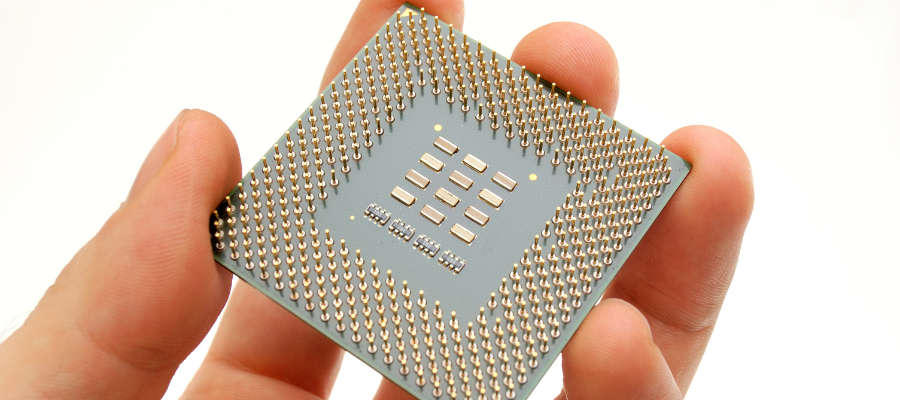
- Package substrate, also known as interposer or substrate, is a specialized type of substrate used in semiconductor packaging.
- Package substrates are typically made of materials such as BT epoxy, ABF (Anisotropic Conductive Film), or ceramics, depending on the specific application requirements.
- They serve as a bridge between semiconductor chips and external electronic systems, providing electrical connections, thermal dissipation, and mechanical support for the chip.
- Package substrates are commonly used in advanced semiconductor packaging technologies such as flip-chip, system-in-package (SiP), and 3D packaging.
Comparative Analysis of PCB and Package Substrate Roles in Electronic Products
- PCBs are used primarily in electronic products where discrete components are mounted and interconnected on a rigid board, such as computers, smartphones, and consumer electronics.
- Package substrates, on the other hand, are integral components of semiconductor packages used in advanced electronic devices such as microprocessors, memory chips, and system-on-chip (SoC) devices.
- PCBs focus on providing electrical connectivity and mechanical support for discrete components, while package substrates focus on providing electrical connections, thermal management, and miniaturization for semiconductor chips.
- While PCBs are typically designed with standard fabrication processes and materials, package substrates often require specialized materials and manufacturing techniques to meet the stringent requirements of semiconductor packaging.
- In terms of complexity, PCBs are generally less complex than package substrates, as they involve simpler routing and interconnect schemes compared to the highly integrated designs of package substrates used in advanced semiconductor packaging technologies.
Case Study Analysis
Case Study of BT Package Substrate Design Using HL832NS Chip
- Overview of the HL832NS Chip: Introduce the HL832NS chip, highlighting its specifications, such as processing power, connectivity options, and thermal requirements.
- Design Considerations: Discuss the key factors considered in selecting BT package substrate for the HL832NS chip, including thermal conductivity, electrical performance, and mechanical stability.
- BT Substrate Design: Describe the specific design features of the BT package substrate tailored for the HL832NS chip, such as the layer stack-up, via structures, and material choices.
- Performance Evaluation: Present the results of performance evaluations, including thermal analysis, signal integrity testing, and reliability assessments, demonstrating the effectiveness of the BT substrate design in meeting the chip’s requirements.
Analysis of Advantages and Limitations of BT Substrate in Practical Applications
- Advantages of BT Substrate: a. High Thermal Conductivity: Discuss how BT substrate’s high thermal conductivity enhances heat dissipation, allowing for efficient thermal management in high-power applications. b. Excellent Electrical Performance: Highlight BT substrate’s superior electrical properties, such as low dielectric loss and signal integrity preservation, contributing to enhanced system performance. c. Mechanical Stability: Emphasize BT substrate’s mechanical robustness, including its resistance to warping, cracking, and delamination, ensuring long-term reliability in harsh environments.
- Limitations of BT Substrate: a. Cost: Address the potentially higher cost of BT substrate compared to conventional FR4 substrates, which may impact the overall manufacturing cost of electronic devices. b. Manufacturing Complexity: Discuss the specialized manufacturing processes and materials required for BT substrate fabrication, which may pose challenges in mass production and supply chain management. c. Application-Specific Considerations: Recognize that the suitability of BT substrate depends on specific application requirements, such as operating temperature range, form factor constraints, and cost considerations.
By conducting a comprehensive case study analysis and evaluating the advantages and limitations of BT substrate in practical applications, stakeholders can make informed decisions regarding substrate selection for their electronic designs, balancing performance, cost, and manufacturability considerations.
FAQs About BT Package Substrate
BT substrate material, also known as bismaleimide-triazine (BT) resin, is a type of high-performance thermosetting polymer used in advanced electronic substrates. It offers excellent thermal stability, mechanical strength, and electrical properties, making it suitable for applications in aerospace, automotive, and telecommunications industries.
The process of manufacturing BT substrate involves several stages:
Material Preparation: Mixing BT epoxy resin with hardeners and additives.
Printing and Stacking: Applying BT epoxy onto Mitsubishi BT laminate sheets and stacking them with copper foils.
Thermal Compression and Curing: Subjecting the laminate stack to heat and pressure to cure the epoxy resin.
Machining and Post-Processing: Precision machining, drilling, and surface treatment to create the final substrate.
The difference between BT substrate and ABF substrate lies in their material composition and application areas:
BT substrate typically consists of layers of BT epoxy resin, Mitsubishi BT laminate, and copper foils. It is used in high-performance electronic applications requiring thermal stability and mechanical strength.
ABF substrate, or Anisotropic Conductive Film, is composed of a base film made of polyimide or polyester with dispersed conductive particles. It is used in flexible electronics and miniaturized electronic assemblies where flexibility and lightweight construction are crucial.
PCB (Printed Circuit Board) and package substrate serve different functions in electronic products:
PCBs provide a rigid platform for mounting and interconnecting discrete electronic components.
Package substrates, on the other hand, facilitate electrical connections, thermal dissipation, and mechanical support for semiconductor chips within advanced packaging technologies like flip-chip and system-in-package (SiP).


发表评论
Want to join the discussion?Feel free to contribute!