
Key Differences Between Lead Frame and Substrate Explained
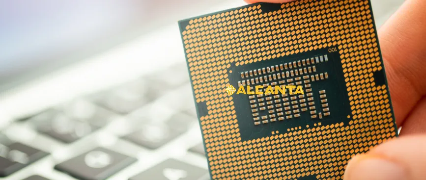
Semiconductor packaging is a crucial aspect of electronic device manufacturing, as it protects sensitive components and ensures reliable electrical connections. Proper packaging enhances performance, thermal management, and durability, playing a significant role in the overall functionality of integrated circuits (ICs). Among various packaging methods, Lead Frames and Substrates are two widely used components.
Lead Frames serve as conductive pathways that connect the semiconductor chip to external circuitry, providing mechanical support and facilitating electrical signals. They are typically made from metal and are essential in traditional package types like dual in-line packages (DIPs).
On the other hand, Substrates offer a platform for mounting chips, incorporating additional circuitry and thermal dissipation features. They come in various forms, including IC Substrates and Package Substrates, each designed to meet specific performance requirements. Understanding the distinctions and applications of Lead Frames and Substrates is vital for optimizing semiconductor packaging solutions.
Definition of Lead Frame
Composition and Function of the Lead Frame
A Lead Frame is primarily composed of a metal alloy, typically copper or nickel, which provides excellent electrical conductivity and mechanical strength. The frame is designed with multiple leads, or pins, that extend from the semiconductor package, allowing for connection to the printed circuit board (PCB) or other electronic components. The main function of the Lead Frame is to establish electrical pathways between the chip and the external environment, facilitating signal transmission while also providing structural support for the encapsulated chip.
Role of Lead Frame in IC Packaging
In integrated circuit (IC) packaging, the Lead Frame plays a vital role by ensuring the reliability and efficiency of electrical connections. It acts as a bridge between the fragile semiconductor die and the PCB, which is crucial for maintaining signal integrity. The design of the Lead Frame also influences thermal management, as it can help dissipate heat generated by the IC during operation. Its ability to provide both mechanical and electrical stability is essential for the overall performance of electronic devices.
Materials and Design Considerations for Lead Frame
Lead Frames are typically made from conductive metals that offer low resistance and high durability. Copper is favored for its excellent conductivity, while nickel may be used for corrosion resistance. Design considerations include the thickness of the leads, spacing between pins, and the overall geometry of the frame to ensure compatibility with various package types. Additionally, manufacturers must consider the thermal expansion characteristics of the materials to prevent stress during temperature fluctuations, thereby ensuring long-term reliability and performance in end-use applications.
Definition of Substrate
Role of Substrate in Semiconductor Packaging
The substrate is a foundational component in semiconductor packaging, serving multiple crucial functions. It provides a stable platform for mounting the semiconductor chip, facilitating secure adhesion and mechanical support. Additionally, substrates integrate various electrical pathways and can incorporate passive components, enabling signal distribution and management. They also play a vital role in thermal dissipation, helping to manage heat generated during device operation, which is essential for maintaining performance and reliability.
Different Types of Substrate
There are several types of substrates, each tailored for specific applications within the semiconductor industry:
1. IC Substrate: Primarily used for integrated circuits, these substrates support chip mounting and include routing layers for electrical connections.
2. Package Substrate: These are designed for specific packaging configurations and often integrate features for enhanced signal integrity and power distribution.
3. Embedded Trace Substrate: This type integrates circuit traces within the substrate material itself, reducing the size and enhancing the performance of high-density applications, particularly useful in advanced packaging technologies.
Material Properties and Applications of Substrate
Substrates are made from a variety of materials, including organic laminates, ceramics, and advanced composite materials. Each material offers unique properties:
– Organic Laminates: Commonly used for their cost-effectiveness and ease of processing. They provide good electrical insulation and are suitable for standard applications.
– Ceramic Substrates: Known for their high thermal conductivity and reliability in extreme environments, these are often used in high-performance and high-reliability applications.
– Composite Materials: These substrates combine the benefits of different materials, optimizing performance for specific applications, such as high-frequency or high-power devices.
Understanding these types and properties is essential for selecting the appropriate substrate for specific semiconductor packaging needs, ensuring optimal device performance and longevity.
Comparison between Lead Frame and Substrate
Differences in Design and Manufacturing Processes
The design and manufacturing processes for Lead Frames and Substrates differ significantly. Lead Frames are typically fabricated from metal, such as copper or alloy, using stamping or etching processes to create intricate patterns that facilitate electrical connections. The design emphasizes simplicity and efficiency, allowing for easy integration into traditional IC packages.
In contrast, Substrates are more complex and can be made from various materials, including organic laminates and ceramics. Their manufacturing process involves layering, lamination, and sometimes photolithography to create multiple layers that integrate circuit paths and passive components. The design of Substrates focuses on optimizing electrical performance, thermal management, and mechanical stability.
Functional Distinctions: Electrical Connections vs. Support Structure
Functionally, Lead Frames primarily serve as the medium for electrical connections. They provide the necessary pathways for signals and power to reach the chip while also offering mechanical support. Their structure is designed to facilitate easy interfacing with circuit boards and other components.
Substrates, on the other hand, serve as both support structures and electrical interconnects. They not only mount the semiconductor chip but also house additional circuitry, which can enhance signal routing and power distribution. Substrates often include features that improve thermal performance, making them essential in high-power applications.
Applicable Scenarios: When to Choose Lead Frame and When to Opt for Substrate
The choice between Lead Frame and Substrate depends on specific application requirements. Lead Frames are ideal for traditional, low-cost IC packaging where simplicity and high-volume production are priorities. They are commonly used in consumer electronics and standard devices.
Substrates are preferable for advanced applications requiring high performance, such as in telecommunications, automotive, and high-frequency devices. When thermal management and signal integrity are critical, Substrates provide the necessary features to ensure reliable operation. Therefore, selecting between Lead Frame and Substrate involves assessing the trade-offs between cost, complexity, and performance needs specific to the intended application.
Integration of Lead Frame and Substrate in IC Packaging
How Both Are Used Together in Actual Packaging
In modern semiconductor packaging, Lead Frames and Substrates can be integrated to leverage the strengths of both components. This integration often occurs in hybrid packaging solutions where the Lead Frame provides the necessary electrical connections and mechanical support, while the Substrate enhances thermal management and signal integrity. The Lead Frame is typically bonded to the substrate using wire bonding or flip-chip techniques, creating a reliable pathway for electrical signals between the chip and external circuitry.
In such configurations, the Lead Frame helps maintain the structural integrity of the package, while the Substrate allows for more complex routing and integration of additional components, such as capacitors or inductors, which can be embedded directly into the substrate material.
Case Study: Real-World Applications of Combining Lead Frame and Substrate
One prominent example of integrating Lead Frames and Substrates is found in automotive electronics. In these applications, high reliability and durability are critical due to the harsh operating environments. A hybrid package combining a metal Lead Frame with a ceramic Substrate has been successfully utilized in power management ICs, which require efficient thermal dissipation and robust electrical performance.
Another application is in RF (radio frequency) devices, where both components are used to manage high-frequency signals effectively. The Lead Frame provides low-resistance paths for RF signals, while the Substrate facilitates the integration of passive components and complex circuitry, reducing the overall footprint of the device.
By using both Lead Frames and Substrates, manufacturers can achieve higher performance, enhanced thermal characteristics, and improved reliability, making these hybrid solutions increasingly popular in advanced semiconductor packaging applications.
Future Trends
New Advancements in Semiconductor Packaging Technology
The semiconductor packaging industry is experiencing rapid advancements driven by the need for miniaturization, enhanced performance, and improved thermal management. Innovations such as 3D packaging, System-in-Package (SiP), and Chiplet architectures are becoming increasingly prominent. These technologies allow for higher density integration of multiple chips within a single package, significantly reducing the footprint and enabling more complex functionalities.
Additionally, advancements in materials science are leading to the development of new substrate materials that offer better electrical performance, lower thermal conductivity, and improved reliability under varying environmental conditions. For instance, organic substrates are being enhanced with embedded components, while ceramic substrates are being optimized for high-frequency applications.
Potential Development Directions for Lead Frame and Substrate
As semiconductor packaging continues to evolve, Lead Frames and Substrates are also expected to adapt to meet emerging demands. For Lead Frames, innovations may focus on reducing the size while maintaining structural integrity and electrical performance. This could involve the use of advanced materials and manufacturing techniques, such as laser processing, which allows for more intricate designs without compromising reliability.
For Substrates, future developments may include the integration of advanced thermal management features, such as embedded heat spreaders or phase-change materials that can adapt to varying thermal loads. Additionally, the trend toward greater integration of passive components directly within the substrate will likely continue, enhancing functionality while minimizing the overall package size.
Furthermore, as the industry moves toward more sustainable practices, there may be an increased focus on environmentally friendly materials and processes for both Lead Frames and Substrates, promoting a greener approach to semiconductor packaging.
In summary, the future of semiconductor packaging will likely see continued innovation in both Lead Frame and Substrate technologies, driven by the need for higher performance, increased functionality, and sustainability in electronics manufacturing.
FAQs about lead frame vs substrate
A lead frame is a metal structure that provides electrical connections and mechanical support for semiconductor devices in packaging.
A substrate in packaging is a base material that supports the semiconductor chip and facilitates electrical connections and thermal management.
The substrate in a semiconductor is the foundational layer that houses the active components and provides a platform for mounting and connecting integrated circuits.
A substrate is primarily used for mounting chips and routing signals, while an interposer is a specialized layer that connects multiple chips, often allowing for higher integration and performance.

