
Understanding Different Types of Insulating Substrates
Insulating substrates play a crucial role in electronic and microelectronic applications by providing electrical isolation and mechanical support for components. These substrates, including materials like HTCC, LTCC, PI, and PTFE, are essential in diverse industries due to their thermal stability and dielectric properties. Electron beam lithography (EBL) further enhances their utility by enabling precise patterning at micro- and nanoscales, crucial for manufacturing high-density electronic circuits and advanced sensors. EBL’s capability to achieve intricate patterns on insulating substrates makes it indispensable in modern semiconductor fabrication and emerging fields like microfluidics. This combination of materials and technology underscores their pivotal role in driving innovation across various electronic devices and systems.
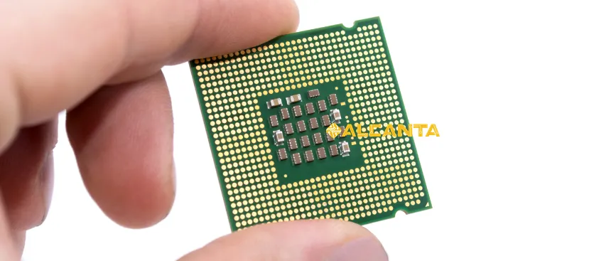
Types of Insulating Substrates
High Temperature Co-Fired Ceramic (HTCC) and Low Temperature Co-Fired Ceramic (LTCC)
High Temperature Co-Fired Ceramic (HTCC) and Low Temperature Co-Fired Ceramic (LTCC) are advanced ceramic materials used extensively in electronics for their excellent thermal and mechanical properties. HTCC involves firing at high temperatures (typically above 1000°C), which results in dense, robust substrates capable of withstanding harsh environments and high frequencies. LTCC, on the other hand, is fired at lower temperatures (around 850°C), allowing integration of conductive and non-conductive layers with precision, suitable for compact, multi-layered designs.
Common Insulating Materials
– Polyimide (PI): Known for its high temperature resistance, flexibility, and excellent dielectric strength, PI is widely used in flexible circuit boards and applications requiring thermal stability.
– Polytetrafluoroethylene (PTFE): PTFE, famous for its non-stick properties, is also an excellent insulator due to its low dielectric constant and high chemical resistance. It finds applications in high-frequency circuit boards and microwave applications.
Understanding these materials is essential for selecting the right substrate based on specific application requirements, ensuring optimal performance and reliability in electronic systems.
Overview of Electron Beam Lithography (EBL)
Principles and Workflow of Electron Beam Lithography
Electron beam lithography (EBL) is a sophisticated nanofabrication technique used to create intricate patterns on substrates at microscopic scales. It operates by directing a focused beam of electrons onto a resist-coated substrate. The key steps involve:
– Beam Generation and Control: Electrons are emitted from a source and controlled using electromagnetic lenses to focus them onto the substrate.
– Resist Coating: A thin layer of resist material is deposited on the substrate’s surface.
– Pattern Exposure: The electron beam selectively exposes the resist, defining the desired pattern with high precision.
– Development: After exposure, the resist is developed to reveal the pattern, which can then be transferred to the substrate through etching or deposition processes.
Applications in Semiconductor Manufacturing and Nanofabrication
EBL plays a pivotal role in:
– Semiconductor Device Fabrication: Used to create nanostructures, transistor gates, and interconnects with sub-micron precision, essential for high-performance integrated circuits.
– Nanotechnology: Enables the fabrication of nano-scale devices such as sensors, photonics components, and biological interfaces, driving advancements in fields like medicine and energy.
EBL’s capability to achieve ultra-high resolution and intricate patterns makes it indispensable for pushing the boundaries of modern electronics and emerging technologies.
Advantages of Electron Beam Lithography on Insulating Substrates
Electron beam lithography (EBL) offers several distinct advantages when used on insulating substrates, making it a preferred choice for various high-tech applications:
High Resolution and Precision Capabilities
EBL operates with electron beams that can achieve extremely fine resolutions, down to sub-nanometer scales. This capability allows for the creation of intricate patterns and features with exceptional detail and accuracy. In comparison to other lithographic techniques, EBL excels in defining small, precise structures essential for advanced electronic devices and microsystems.
Suitable for Complex Structures and Small Feature Sizes
Insulating substrates often require precise patterning of complex structures and small feature sizes to accommodate intricate circuit designs and microelectronic components. EBL’s ability to handle these requirements efficiently makes it ideal for fabricating high-density integrated circuits, MEMS (Micro-Electro-Mechanical Systems), and nanoscale devices. Its versatility in creating custom patterns on diverse materials like HTCC, LTCC, PI, and PTFE underscores its importance in modern semiconductor manufacturing and nanofabrication.
These advantages position EBL as a crucial technology for driving innovation in electronics, enabling the development of next-generation devices with enhanced performance and functionality.
Typical Application Scenarios
Electron beam lithography (EBL) on insulating substrates finds diverse applications across various high-tech fields, showcasing its versatility and precision:
Manufacturing of Microelectronic Devices
EBL plays a crucial role in the fabrication of microelectronic devices such as integrated circuits (ICs), where it enables the creation of intricate patterns on insulating substrates. This capability is essential for producing transistor gates, interconnects, and other critical components with sub-micron precision. EBL’s ability to define ultra-small features ensures the miniaturization and performance enhancement of electronic devices, meeting the demands of modern technology.
Research and Development of Sensors and Microfluidic Devices
In sensor development, EBL facilitates the creation of nano-scale structures that are crucial for sensing elements, enhancing sensitivity and specificity. Insulating substrates like PI and PTFE are particularly suited for sensor applications due to their chemical resistance and thermal stability. Moreover, EBL enables the fabrication of microfluidic devices used in biomedical research and diagnostics, where precise control over fluid flow and reaction chambers is essential.
These applications underscore EBL’s importance in advancing microelectronics, sensors, and microfluidics, driving innovations that benefit fields ranging from healthcare to telecommunications.
Market Trends and Future Outlook
Development Trends in Insulating Substrate Technology
The field of insulating substrates is witnessing significant advancements driven by technological innovations and market demands:
– Advanced Materials: Research continues to focus on developing insulating materials with enhanced thermal conductivity, lower dielectric loss, and improved mechanical properties. Materials like HTCC and LTCC are evolving to support higher frequencies and complex circuit designs.
– Integration with Emerging Technologies: Insulating substrates are increasingly integrated with emerging technologies such as IoT (Internet of Things), 5G communications, and AI (Artificial Intelligence). These substrates enable the miniaturization and performance optimization of electronic components essential for these applications.
Potential Impact on Future Electronics and Emerging Technologies
Insulating substrates, coupled with electron beam lithography (EBL), are poised to shape the future of electronics in several ways:
– Miniaturization and Integration: EBL’s ability to create intricate patterns on insulating substrates supports the miniaturization of electronic devices, enhancing their functionality and performance.
– Enhanced Functionality: The precise patterning capabilities of EBL enable the development of advanced sensors, microfluidic devices, and biomedical implants that rely on compact, high-performance electronics.
– Insulating substrates contribute to improving energy efficiency in electronics by reducing signal loss and enabling higher operating frequencies, crucial for power-sensitive applications.
As technology continues to advance, insulating substrates and EBL will play pivotal roles in driving innovation across diverse industries, from healthcare and telecommunications to automotive and aerospace. Their continued development and integration into new applications promise to revolutionize how electronics are designed, manufactured, and utilized in the future.
FAQs about insulating substrate
Common types include High Temperature Co-Fired Ceramic (HTCC), Low Temperature Co-Fired Ceramic (LTCC), Polyimide (PI), and Polytetrafluoroethylene (PTFE). Each type has specific properties suited for different applications.
Insulating substrates offer high dielectric strength, thermal stability, and resistance to chemicals. They enable miniaturization of electronic components and support advanced manufacturing processes like electron beam lithography (EBL).
They are used as base materials for PCBs (Printed Circuit Boards), in packaging substrates for ICs (Integrated Circuits), and in various high-frequency applications where electrical isolation and signal integrity are critical.
EBL is a nanofabrication technique that uses a focused beam of electrons to create patterns on substrates. It is particularly effective on insulating substrates due to their ability to withstand high precision patterning and small feature sizes.

