
Excellence in Flip Chip RF Substrate Manufacturing
Flip Chip technology represents a significant advancement in semiconductor packaging, offering a compact and high-performance solution for various electronic devices. Its applications extend to the realm of Radio Frequency (RF) packaging, where demands for enhanced performance and miniaturization are paramount. In this context, the role of Flip Chip RF Package Substrates Manufacturer products becomes indispensable. These products serve as the backbone for efficient RF signal transmission, ensuring minimal signal loss and optimal performance. As RF devices continue to proliferate across industries such as telecommunications, automotive, and aerospace, the importance of reliable and high-quality Flip Chip RF Package Substrates becomes increasingly evident. This blog explores the critical role of these substrates in facilitating seamless RF communication and the pivotal contributions of manufacturers in driving innovation within this domain.
Overview of Flip Chip Packaging Technology
Basic Principles and Working Mechanisms:
Flip Chip packaging technology involves the direct attachment of semiconductor chips to substrates or carriers, with the active side facing down. This is achieved through the use of tiny solder bumps or balls that serve as electrical connections between the chip and the substrate. The process typically involves precise alignment of the chip and substrate followed by controlled heating to melt the solder and create reliable connections. Unlike traditional wire bonding, which involves bonding wires from the chip to the substrate, Flip Chip technology eliminates the need for wire loops, enabling higher density interconnects and shorter signal paths.
Advantages in RF Applications:
Flip Chip packaging offers several advantages that are particularly beneficial in RF applications. Firstly, it allows for higher operating frequencies due to reduced parasitic capacitance and inductance, resulting in improved signal integrity and higher data transmission rates. Additionally, the direct connection between the chip and substrate leads to lower resistance, minimizing signal loss and improving overall efficiency. Furthermore, Flip Chip technology enables better thermal management by providing a direct thermal path from the chip to the substrate, enhancing heat dissipation and ensuring reliable performance even in high-power RF applications.
Components of Flip Chip Packaging
Introduction to Basic Components:
Flip Chip packaging comprises several essential components that collectively enable its functionality. Firstly, the semiconductor chip itself forms the core of the package, containing the integrated circuits and other electronic components. The substrate, often made of materials like silicon, organic laminate, or ceramics, provides a stable foundation for the chip and facilitates electrical connections. Packaging materials, such as solder bumps or conductive adhesives, are used to attach the chip to the substrate and create electrical pathways. Additionally, underfill materials may be applied to enhance mechanical stability and protect the solder joints from mechanical stress.
Special Requirements in RF Applications:
In RF applications, specific considerations must be taken into account when designing Flip Chip packaging. High-frequency transmission lines demand precise impedance matching and controlled signal propagation to minimize reflections and ensure signal integrity. Therefore, substrates with low dielectric constant and loss tangent are preferred to minimize signal attenuation. Moreover, good thermal conduction is crucial to dissipate heat generated during high-frequency operation effectively. Thus, substrates with high thermal conductivity, such as metal-core or ceramic substrates, are often utilized to enhance thermal management and maintain device reliability in RF applications.
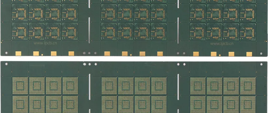
Substrates in Flip Chip Packaging
Role and Importance of Substrates:
Substrates play a crucial role in Flip Chip packaging, serving as the foundation for semiconductor chips and providing electrical connections between the chips and the external environment. They facilitate the transmission of signals, power, and heat between the chip and the rest of the system. The choice of substrate material and manufacturing processes directly impact the performance, reliability, and cost-effectiveness of the packaged device.
Key Points in Substrate Selection:
1. Material Selection: Substrates for Flip Chip packaging are typically chosen based on factors such as electrical properties, thermal conductivity, mechanical strength, and cost. Common materials include organic laminate (e.g., FR-4), ceramic (e.g., alumina or aluminum nitride), and metal-core substrates (e.g., aluminum or copper).
2. Electrical Properties: In RF applications, substrates with low dielectric constant and low loss tangent are preferred to minimize signal attenuation and distortion. This ensures high-speed signal transmission and maintains signal integrity.
3. Thermal Management: Effective heat dissipation is essential for maintaining device reliability, especially in high-power RF applications. Substrates with high thermal conductivity help to efficiently transfer heat away from the chip, preventing overheating and thermal damage.
4. Manufacturing Processes: The manufacturing processes for substrates include techniques such as PCB fabrication, thin-film deposition, etching, and plating. Advanced processes like laser drilling and microvia technology enable the creation of high-density interconnects and complex circuitry on the substrate.
5. Reliability and Cost: Substrate design and fabrication must balance performance requirements with cost considerations. High-reliability substrates undergo rigorous testing to ensure durability under various operating conditions, while cost-effective solutions optimize material usage and manufacturing efficiency.
Overall, the selection and design of substrates in Flip Chip packaging are critical factors that directly influence the performance, reliability, and manufacturability of RF devices.
Flip Chip RF Package Substrates Manufacturer: Samsung Electro-Mechanics
Brief Introduction:
Samsung Electro-Mechanics is a leading manufacturer in the field of electronic components and materials, with a strong focus on Flip Chip RF Package Substrates. Leveraging decades of experience and expertise, Samsung Electro-Mechanics has established itself as a key player in the semiconductor packaging industry. The company’s commitment to innovation and quality has earned it a reputation for excellence in providing advanced solutions for RF applications.
Position in the Field:
Samsung Electro-Mechanics occupies a prominent position in the Flip Chip RF Package Substrates manufacturing sector. With state-of-the-art facilities and a dedicated team of engineers, the company is at the forefront of developing cutting-edge technologies and solutions to meet the evolving demands of the RF market. Its comprehensive product portfolio caters to a wide range of RF applications, including wireless communication, automotive radar, and IoT devices.
Professional Capabilities and Technological Advantages:
1. Advanced Manufacturing Processes: Samsung Electro-Mechanics utilizes advanced manufacturing processes and equipment to ensure the highest level of precision and quality in its products. From substrate fabrication to assembly and testing, the company employs stringent quality control measures to deliver reliable and consistent performance.
2. Innovative Materials: The company invests heavily in research and development to develop innovative materials optimized for RF packaging applications. These materials offer superior electrical and thermal properties, enabling enhanced signal transmission, reduced power consumption, and improved reliability in RF devices.
3. Customization and Flexibility: Samsung Electro-Mechanics works closely with customers to understand their specific requirements and provide customized solutions tailored to their needs. Whether it’s substrate design, material selection, or packaging configuration, the company offers flexibility to accommodate diverse application needs and performance goals.
4. Global Reach and Support: With a global network of manufacturing facilities, sales offices, and technical support centers, Samsung Electro-Mechanics provides comprehensive support to customers worldwide. Its extensive distribution network ensures timely delivery of products and services, while its dedicated technical teams offer expert guidance and assistance throughout the product lifecycle.
In conclusion, Samsung Electro-Mechanics stands as a trusted partner for Flip Chip RF Package Substrates, offering unparalleled expertise, innovation, and support to drive the advancement of RF technology across industries.
Material Selection in Flip Chip Packaging
Chip Bonding Material Selection and Characteristics:
In Flip Chip packaging, the material used for chip bonding plays a critical role in ensuring reliable electrical connections between the semiconductor chip and the substrate. The chosen bonding material must exhibit several key characteristics to meet the requirements of high-performance electronic devices. These characteristics include:
1. Electrical Conductivity: The bonding material should possess high electrical conductivity to enable efficient transmission of signals between the chip and the substrate. This ensures minimal signal loss and optimal performance of the packaged device.
2. Thermal Conductivity: Effective heat dissipation is essential for maintaining device reliability, especially in RF applications where thermal management is crucial. Therefore, the bonding material should have good thermal conductivity to facilitate the efficient transfer of heat away from the chip.
3. Mechanical Strength: The bonding material must provide robust mechanical support to withstand thermal cycling, mechanical stress, and environmental factors without compromising the integrity of the electrical connections. High mechanical strength ensures long-term reliability and durability of the packaged device.
4. Compatibility: The bonding material should be compatible with both the chip and the substrate materials to ensure proper adhesion and compatibility with the surrounding packaging materials. Compatibility issues can lead to delamination, solder joint failure, or other reliability issues.
5. Reliability: The bonding material should exhibit stable electrical and mechanical properties over a wide range of operating conditions, including temperature fluctuations, humidity, and mechanical shock. This ensures the long-term reliability and performance of the packaged device in various application environments.
Commonly Used Material Types:
Several material types are commonly used for chip bonding in Flip Chip packaging, each offering unique advantages and characteristics:
1. Solder Bumps: Solder bumps, typically composed of lead-free alloys such as SAC (tin-silver-copper) or SnAgCu, are widely used for chip bonding due to their excellent electrical and mechanical properties. Solder bumps provide reliable electrical connections and facilitate the reflow soldering process during assembly.
2. Conductive Adhesives: Conductive adhesives, consisting of conductive particles dispersed in a polymer matrix, offer an alternative bonding solution for Flip Chip packaging. These adhesives provide flexibility in bonding non-flat or irregular surfaces and can be applied using various methods such as dispensing or printing.
3. Gold Stud Bumps: Gold stud bumps, formed by electroplating or wire bonding gold wires onto the chip pads, are sometimes used in specialized applications requiring ultra-fine pitch interconnects or high-reliability connections. Gold stud bumps offer excellent electrical conductivity and reliability but may involve higher manufacturing costs.
4. Copper Pillar Bumps: Copper pillar bumps, formed by electroplating copper onto the chip pads, are increasingly used in advanced Flip Chip packaging technologies such as 3D integration and system-in-package (SiP) solutions. Copper pillar bumps offer superior electrical and thermal performance, enabling higher interconnect densities and improved signal integrity.
In summary, the selection of bonding materials in Flip Chip packaging is a critical consideration that directly impacts the performance, reliability, and manufacturability of electronic devices. Each material type offers unique advantages and characteristics, allowing designers to tailor their choices to meet the specific requirements of their applications.
FAQs about Flip Chip RF Package Substrates Manufacturer
The substrate of the flip chip package can vary depending on the specific application and requirements. Common substrate materials include organic laminate (such as FR-4), ceramic (such as alumina or aluminum nitride), and metal-core substrates (such as aluminum or copper).
The material used for flip chip bonding typically includes solder bumps or conductive adhesives. Solder bumps are often composed of lead-free alloys like SAC (tin-silver-copper) or SnAgCu, while conductive adhesives consist of conductive particles dispersed in a polymer matrix.
Substrates for semiconductor packaging encompass a wide range of materials tailored to meet different performance and application needs. These materials include organic laminates, ceramics, metal-core substrates, silicon, glass, and specialized materials like silicon carbide (SiC) or gallium arsenide (GaAs).
The components of a flip chip typically include the semiconductor chip itself, the substrate, packaging materials (such as solder bumps or conductive adhesives), and possibly underfill materials for mechanical stability and protection of solder joints. Additionally, advanced flip chip designs may incorporate features like redistribution layers, dielectric layers, and passivation layers to enhance performance and reliability.

