
Navigating Flip Chip BGA Substrate Selection
In the realm of electronic packaging, Flip Chip BGA Substrate stands as a pivotal innovation. Flip chip and BGA (Ball Grid Array) technologies revolutionize how electronic components are interconnected and packaged within devices. Flip chip technology involves the direct mounting of semiconductor chips onto substrates, utilizing solder bumps for electrical connections, while BGA employs a grid of solder balls beneath the chip for the same purpose. These advanced packaging methods are indispensable in modern electronics, facilitating compact designs, enhanced performance, and improved reliability. From smartphones to automotive electronics, flip chip BGA substrates find widespread applications across various industries, driving efficiency and enabling the realization of cutting-edge electronic devices. Understanding the intricacies of these technologies is fundamental for engineers and manufacturers striving to stay at the forefront of innovation in electronic packaging.
Understanding Flip Chip BGA Substrate Process Flow
Flip Chip BGA Process Flow: Step-by-Step Explanation
- Die Preparation: The process begins with preparing the semiconductor die, which involves testing, inspection, and cleaning to ensure quality and reliability. This step is crucial to identify any defects before proceeding further.
- Substrate Preparation: The substrate, typically made of materials like silicon, ceramic, or organic laminate, undergoes surface preparation, including cleaning and application of underfill materials if necessary. This ensures proper adhesion and electrical connectivity.
- Bump Formation: In flip chip technology, solder bumps are formed on the bonding pads of the semiconductor die. This is typically done through processes like electroplating or solder ball placement, creating precise and reliable connections.
- Alignment and Placement: The semiconductor die is precisely aligned and placed onto the substrate using automated machinery. This step requires high accuracy to ensure proper alignment of the solder bumps with the corresponding pads on the substrate.
- Reflow Soldering: Once the die is aligned and placed, the assembly undergoes reflow soldering, where heat is applied to melt the solder bumps, forming solid connections between the die and substrate. This process ensures strong electrical and mechanical bonds.
- Underfill Encapsulation: In some cases, underfill materials are applied to encapsulate the solder joints between the die and substrate. This enhances reliability by reducing mechanical stress and preventing moisture ingress.
Key Stages and Techniques Involved
- Alignment Accuracy: Achieving precise alignment between the solder bumps and substrate pads is critical for reliable electrical connections and optimal performance.
- Soldering Control: Controlling the reflow soldering process is essential to ensure proper melting and solidification of solder bumps, preventing defects like solder bridges or voids.
- Underfill Application: Applying underfill materials requires careful consideration of viscosity, dispensing technique, and curing process to achieve uniform encapsulation and minimize voids or air pockets.
- Quality Inspection: Throughout the process, various quality control measures, including visual inspection, X-ray analysis, and electrical testing, are conducted to detect and rectify any defects or inconsistencies.
Understanding the intricacies of the flip chip BGA substrate process flow is crucial for optimizing manufacturing efficiency, ensuring product quality, and meeting the demands of modern electronic devices.
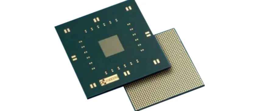
Exploring Flip Chip Ball Grid Array (FC-BGA) Substrate
Flip Chip BGA Substrate: Definition and Characteristics
The Flip Chip Ball Grid Array (FC-BGA) substrate is a critical component in flip chip packaging technology. It serves as the platform for mounting and interconnecting semiconductor dies using flip chip technology. FC-BGA substrates feature an array of solder balls arranged in a grid pattern beneath the semiconductor die, providing electrical connections to the external circuitry.
Material Composition and Properties
FC-BGA substrates are typically fabricated from high-performance materials such as silicon, ceramic, or organic laminate. These materials offer excellent thermal conductivity, electrical insulation, and mechanical stability, crucial for reliable operation in diverse electronic applications. Silicon substrates provide superior thermal management, while ceramic substrates offer high rigidity and durability. Organic laminate substrates, on the other hand, offer cost-effectiveness and flexibility in design.
Comparison with Traditional BGA Substrates
Compared to traditional BGA substrates, FC-BGA substrates offer several distinct advantages. Firstly, FC-BGA substrates enable direct electrical connections between the semiconductor die and substrate, eliminating the need for wire bonding. This results in shorter interconnection lengths, reduced parasitic effects, and improved electrical performance. Additionally, FC-BGA substrates offer higher I/O density, allowing for more compact and feature-rich electronic devices. Moreover, FC-BGA substrates exhibit superior thermal management capabilities, enabling efficient heat dissipation and enhanced reliability in high-power applications.
Understanding the composition, properties, and advantages of FC-BGA substrates is essential for engineers and manufacturers seeking to leverage flip chip technology for advanced electronic packaging solutions. By harnessing the benefits of FC-BGA substrates, designers can achieve higher performance, increased functionality, and greater reliability in their electronic products.
Flip Chip vs. BGA: A Comparative Analysis of Flip Chip BGA Substrate
Differences in Packaging Technology and Architecture
- Flip Chip Technology: In flip chip packaging, the semiconductor die is directly mounted onto the substrate, with electrical connections made using solder bumps. This results in shorter interconnection lengths and reduced parasitic effects, leading to improved electrical performance.
- BGA Technology: Ball Grid Array (BGA) packaging involves mounting the semiconductor die on the substrate, with electrical connections made via an array of solder balls beneath the die. BGA packages typically have longer interconnection lengths compared to flip chip, potentially leading to higher parasitic effects.
Performance Metrics: Speed, Size, and Heat Dissipation
- Speed: Flip chip technology offers higher speed capabilities due to shorter interconnection lengths and reduced parasitic effects. This makes it suitable for high-frequency applications such as microprocessors and high-speed communication devices.
- Size: Flip chip packages tend to be smaller in size compared to BGA packages, thanks to the direct mounting of the die onto the substrate. This compact form factor is advantageous for miniaturized electronic devices where space is limited.
- Heat Dissipation: Flip chip technology provides better heat dissipation compared to BGA due to its direct die-substrate interface, enabling efficient heat transfer away from the semiconductor die. This makes flip chip suitable for high-power applications requiring effective thermal management.
Application Suitability: When to Choose Flip Chip or BGA
- Flip Chip: Ideal for high-performance applications requiring high-speed operation, compact size, and efficient heat dissipation. Common applications include microprocessors, memory devices, and high-speed communication modules.
- BGA: Suitable for applications where cost-effectiveness, ease of assembly, and moderate performance are prioritized. BGA packages are commonly used in consumer electronics, automotive electronics, and industrial control systems.
Understanding the differences in packaging technology, performance metrics, and application suitability between flip chip and BGA is essential for selecting the most appropriate packaging solution for a given electronic device. By carefully evaluating these factors, engineers and designers can optimize performance, reliability, and cost-effectiveness in their electronic designs.
Flip Chip vs. Wire Bond: Contrasting Assembly Techniques
Overview of Wire Bonding in Electronic Packaging
Wire bonding is a traditional method of interconnecting semiconductor chips with external circuitry in electronic packaging. It involves using thin wires made of materials like gold, aluminum, or copper to create electrical connections between the bonding pads on the semiconductor die and the leads or pins on the package substrate. Wire bonding can be performed using either ball bonding or wedge bonding techniques, each offering unique advantages and limitations.
Advantages and Disadvantages Compared to Flip Chip Technology
Advantages of Wire Bonding
- Cost-Effectiveness: Wire bonding is often more cost-effective than flip chip technology, particularly for low- to medium-volume production runs.
- Flexibility: Wire bonding allows for greater flexibility in die placement and package design compared to flip chip, making it suitable for a wide range of electronic devices.
- Reliability: Wire bonding has a long history of proven reliability in various applications, particularly in environments with moderate temperature and mechanical stress.
Disadvantages of Wire Bonding
- Limited Performance: Wire bonding may exhibit higher parasitic effects and lower electrical performance compared to flip chip technology, particularly at high frequencies.
- Size Limitations: Wire bonding may not be suitable for miniaturized electronic devices due to the space required for wire routing and looping.
- Thermal Management: Wire bonding may present challenges in thermal management, as the wires can act as thermal barriers and may be susceptible to damage under high-temperature conditions.
In contrast to wire bonding, flip chip technology offers several distinct advantages, including shorter interconnection lengths, improved electrical performance, and enhanced thermal management. However, flip chip technology may also be associated with higher manufacturing costs and complexity compared to wire bonding, particularly for small-scale production.
Understanding the differences between wire bonding and flip chip technology is essential for selecting the most appropriate assembly technique for a given electronic application. By weighing the advantages and disadvantages of each approach, engineers and manufacturers can optimize performance, reliability, and cost-effectiveness in their electronic packaging designs.
Comparison between FC-BGA and Traditional BGA Packages
When comparing Flip Chip BGA Substrate (FC-BGA) packages with traditional BGA packages, several key factors come into play, influencing structural design, performance, manufacturing considerations, and cost analysis.
Structural Differences and Impact on Performance
- Flip Chip BGA Substrate: FC-BGA packages feature a flip chip architecture where the semiconductor die is directly mounted onto the substrate, with solder bumps providing electrical connections. This direct connection results in shorter interconnection lengths, reduced parasitic effects, and improved electrical performance. Additionally, FC-BGA substrates often incorporate advanced materials and design features to enhance thermal management and reliability.
- Traditional BGA Packages: Traditional BGA packages utilize wire bonding or other interconnection methods to attach the semiconductor die to the substrate. These packages typically have longer interconnection lengths compared to flip chip technology, potentially leading to higher parasitic effects and reduced electrical performance. However, traditional BGA packages may offer advantages in terms of ease of assembly and cost-effectiveness for certain applications.
Manufacturing Considerations and Cost Analysis
- Manufacturing Complexity: Manufacturing FC-BGA packages generally involves more complex processes compared to traditional BGA packages due to the direct die attachment and solder bump formation. This complexity may require specialized equipment and expertise, potentially leading to higher production costs.
- Material Costs: FC-BGA substrates often utilize high-performance materials such as silicon, ceramic, or organic laminate, which may be more expensive compared to the materials used in traditional BGA packages. However, the performance benefits provided by FC-BGA substrates may justify the higher material costs in certain applications.
- Assembly Yield: The assembly yield for FC-BGA packages may vary depending on factors such as solder bump formation, die placement accuracy, and underfill encapsulation. Achieving high assembly yield rates is crucial for minimizing manufacturing costs and ensuring product reliability.
In summary, while FC-BGA packages offer superior electrical performance and thermal management compared to traditional BGA packages, they may also involve higher manufacturing complexity and costs. Engineers and manufacturers must carefully evaluate the trade-offs between performance, manufacturing considerations, and cost analysis when selecting between FC-BGA and traditional BGA packages for a given electronic application.
Understanding the structural differences and manufacturing considerations between FC-BGA and traditional BGA packages is essential for optimizing performance, reliability, and cost-effectiveness in electronic packaging designs.
Substrate Material for Flip Chip
Flip chip technology relies on the selection of appropriate substrate materials to ensure optimal performance, reliability, and manufacturability. A detailed examination of substrate materials used in flip chip technology reveals a range of options, each with unique properties and considerations.
Detailed Examination of Substrate Materials Used in Flip Chip Technology
- Silicon Substrates: Silicon substrates offer excellent thermal conductivity, making them ideal for applications requiring efficient heat dissipation. They also provide high mechanical stability and reliability, making them suitable for high-performance electronic devices such as microprocessors and memory modules.
- Ceramic Substrates: Ceramic substrates, such as alumina (Al2O3) and aluminum nitride (AlN), offer superior thermal performance and reliability compared to organic substrates. They provide excellent electrical insulation, mechanical strength, and thermal conductivity, making them suitable for high-power and high-frequency applications.
- Organic Substrates: Organic substrates, typically made of epoxy or polyimide resin materials, offer cost-effectiveness and flexibility in design. They provide good electrical insulation and ease of fabrication, making them suitable for a wide range of electronic devices, including consumer electronics, automotive systems, and industrial applications.
Factors Influencing Material Selection and Performance
- Electrical Performance: Substrate materials must exhibit low dielectric loss and high electrical insulation to minimize signal attenuation and ensure signal integrity. High-frequency applications may require materials with low dielectric constants and loss tangents to reduce signal distortion.
- Thermal Management: Effective thermal management is crucial in flip chip technology to dissipate heat generated by the semiconductor die. Substrate materials with high thermal conductivity and low thermal resistance help to efficiently transfer heat away from the die, preventing overheating and ensuring long-term reliability.
- Mechanical Stability: Substrate materials must provide sufficient mechanical strength and stability to withstand thermal cycling, mechanical stress, and environmental factors. High-strength materials such as ceramics are preferred for applications requiring ruggedness and reliability.
- Manufacturability: Substrate materials should be compatible with manufacturing processes such as soldering, wire bonding, and assembly. Materials with good solderability, adhesion, and dimensional stability facilitate efficient manufacturing and yield high-quality flip chip assemblies.
- Cost Considerations: Material cost is an important factor in substrate selection, particularly for high-volume production. While materials like silicon and ceramic offer superior performance, they may also be more expensive compared to organic substrates. Cost-effectiveness must be balanced with performance requirements and application needs.
By carefully evaluating these factors, engineers can select the most suitable substrate material for flip chip technology, ensuring optimal performance, reliability, and cost-effectiveness in electronic packaging designs.
FAQs About Flip Chip BGA Substrate
The substrate material commonly used for flip chip technology includes silicon, ceramic, and organic laminate.
The main difference between BGA (Ball Grid Array) and flip chip lies in their packaging technology. BGA involves mounting the semiconductor die on the substrate with solder balls underneath, while flip chip directly mounts the die onto the substrate using solder bumps on the die.
The substrate of BGA typically consists of materials like organic laminate, ceramic, or silicon.
A flip chip component is a semiconductor device where the semiconductor die is directly mounted onto the substrate using solder bumps, facilitating electrical connections without the need for wire bonding.

